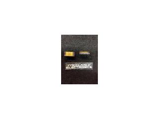
Freelance Electronics Components Distributor
Closed Dec 25th-26th
800-300-1968
We Stock Hard to Find Parts

AD5323BRU

Part # AD5323BRU
Description DAC 2CH RES-STRING 12-BIT 16TSSOP - Rail/Tube
Category IC
Availability In Stock
Qty 33
Qty Price
1 - 6 $29.61870
7 - 13 $23.56033
14 - 20 $22.21403
21 - 27 $20.64334
28 + $18.39950
Manufacturer Available Qty
Analog Devices
Date Code: 0411
  • Shipping Freelance Stock: 10
    Ships Immediately
Analog Devices
Date Code: 0417
  • Shipping Freelance Stock: 23
    Ships Immediately


Technical Document


DISCLAIMER: The information provided herein is solely for informational purposes. Customers must be aware of the suitability of this product for their application, and consider that variable factors such as Manufacturer, Product Category, Date Codes, Pictures and Descriptions may differ from available inventory.

REV. 0
Information furnished by Analog Devices is believed to be accurate and
reliable. However, no responsibility is assumed by Analog Devices for its
use, nor for any infringements of patents or other rights of third parties
which may result from its use. No license is granted by implication or
otherwise under any patent or patent rights of Analog Devices.
a
AD5303/AD5313/AD5323*
One Technology Way, P.O. Box 9106, Norwood, MA 02062-9106, U.S.A.
Tel: 781/329-4700 World Wide Web Site: http://www.analog.com
Fax: 781/326-8703 © Analog Devices, Inc., 1999
+2.5 V to +5.5 V, 230 A, Dual Rail-to-Rail
Voltage Output 8-/10-/12-Bit DACs
FUNCTIONAL BLOCK DIAGRAM
BUFFER
POWER-DOWN
LOGIC
RESISTOR
NETWORK
STRING
DAC
AD5303/AD5313/AD5323
V
OUT
A
V
OUT
B
V
DD
V
REF
A
V
REF
B
DAC
REGISTER
DAC
REGISTER
>
SYNC
SCLK
DIN
GND
BUF A
SDO
CLR
BUF B
STRING
DAC
DCEN
LDAC
POWER-ON
RESET
PD
BUFFER
GAIN-SELECT
LOGIC
RESISTOR
NETWORK
INPUT
REGISTER
INPUT
REGISTER
INTERFACE
LOGIC
FEATURES
AD5303: Two Buffered 8-Bit DACs in One Package
AD5313: Two Buffered 10-Bit DACs in One Package
AD5323: Two Buffered 12-Bit DACs in One Package
16-Lead TSSOP Package
Micropower Operation: 300 A @ 5 V (Including
Reference Current)
Power-Down to 200 nA @ 5 V, 50 nA @ 3 V
+2.5 V to +5.5 V Power Supply
Double-Buffered Input Logic
Guaranteed Monotonic By Design Over All Codes
Buffered/Unbuffered Reference Input Options
Output Range: 0–V
REF
or 0–2 V
REF
Power-On-Reset to Zero Volts
SDO Daisy-Chaining Option
Simultaneous Update of DAC Outputs via LDAC Pin
Asynchronous CLR Facility
Low Power Serial Interface with Schmitt-Triggered
Inputs
On-Chip Rail-to-Rail Output Buffer Amplifiers
APPLICATIONS
Portable Battery Powered Instruments
Digital Gain and Offset Adjustment
Programmable Voltage and Current Sources
Programmable Attenuators
GENERAL DESCRIPTION
The AD5303/AD5313/AD5323 are dual 8-, 10- and 12-bit
buffered voltage output DACs in a 16-lead TSSOP package that
operate from a single +2.5 V to +5.5 V supply consuming 230 µA
at 3 V. Their on-chip output amplifiers allow the outputs to
swing rail-to-rail with a slew rate of 0.7 V/µs. The AD5303/
AD5313/AD5323 utilize a versatile 3-wire serial interface that
operates at clock rates up to 30 MHz and is compatible with
standard SPI™, QSPI, MICROWIRE™ and DSP interface
standards.
The references for the two DACs are derived from two reference
pins (one per DAC). These reference inputs may be configured
as buffered or unbuffered inputs. The parts incorporate a power-
on-reset circuit that ensures that the DAC outputs power-up to
0 V and remain there until a valid write to the device takes place.
There is also an asynchronous active low CLR pin that clears
both DACs to 0 V. The outputs of both DACs may be updated
simultaneously using the asynchronous LDAC input. The
parts contain a power-down feature that reduces the current
consumption of the devices to 200 nA at 5 V (50 nA at 3 V) and
provides software-selectable output loads while in power-down
mode. The parts may also be used in daisy-chaining applications
using the SDO pin.
The low power consumption of these parts in normal operation
make them ideally suited to portable battery operated equip-
ment. The power consumption is 1.5 mW at 5 V, 0.7 mW at
3 V, reducing to 1 µW in power-down mode.
*Protected by U.S. Patent No. 5684481; other patents pending.
SPI is a trademark of Motorola, Inc.
MICROWIRE is a trademark of National Semiconductor Corporation.
REV. 0
–2–
AD5303/AD5313/AD5323–SPECIFICATIONS
(V
DD
= +2.5 V to +5.5 V; V
REF
= +2 V; R
L
= 2 k to GND; C
L
= 200 pF to GND; all specifications T
MIN
to T
MAX
unless otherwise noted.)
B Version
2
Parameter
1
Min Typ Max Units Conditions/Comments
DC PERFORMANCE
3, 4
AD5303
Resolution 8 Bits
Relative Accuracy ± 0.15 ± 1 LSB
Differential Nonlinearity ± 0.02 ± 0.25 LSB Guaranteed Monotonic by Design Over All Codes
AD5313
Resolution 10 Bits
Relative Accuracy ± 0.5 ± 3 LSB
Differential Nonlinearity ± 0.05 ± 0.5 LSB Guaranteed Monotonic by Design Over All Codes
AD5323
Resolution 12 Bits
Relative Accuracy ± 2 ± 12 LSB
Differential Nonlinearity ± 0.2 ± 1 LSB Guaranteed Monotonic by Design Over All Codes
Offset Error ± 0.4 ± 3 % of FSR See Figures 3 and 4
Gain Error ± 0.15 ± 1 % of FSR See Figures 3 and 4
Lower Deadband 10 60 mV See Figures 3 and 4
Offset Error Drift
5
–12 ppm of FSR/°C
Gain Error Drift
5
–5 ppm of FSR/°C
Power Supply Rejection Ratio
5
–60 dB V
DD
= ±10%
DC Crosstalk
5
30 µV
DAC REFERENCE INPUTS
5
V
REF
Input Range 1 V
DD
V Buffered Reference Mode
0V
DD
V Unbuffered Reference Mode
V
REF
Input Impedance >10 M Buffered Reference Mode
180 k Unbuffered Reference Mode. 0–V
REF
Output Range,
Input Impedance = R
DAC
90 k Unbuffered Reference Mode. 0–2 V
REF
Output Range,
Input Impedance = R
DAC
Reference Feedthrough –90 dB Frequency = 10 kHz
Channel-to-Channel Isolation –80 dB Frequency = 10 kHz
OUTPUT CHARACTERISTICS
5
Minimum Output Voltage
6
0.001 V mi
n This is a measure of the minimum and maximum
Maximum Output Voltage
6
V
DD
0.001 V max drive capability of the output amplifier.
DC Output Impedance 0.5
Short Circuit Current 50 mA V
DD
= +5 V
20 mA V
DD
= +3 V
Power-Up Time 2.5 µs Coming Out of Power-Down Mode. V
DD
= +5 V
5 µs Coming Out of Power-Down Mode. V
DD
= +3 V
LOGIC INPUTS
5
Input Current ± 1 µA
V
IL
, Input Low Voltage 0.8 V V
DD
= +5 V ± 10%
0.6 V V
DD
= +3 V ± 10%
0.5 V V
DD
= +2.5 V
V
IH
, Input High Voltage 2.4 V V
DD
= +5 V ± 10%
2.1 V V
DD
= +3 V ± 10%
2.0 V V
DD
= +2.5 V
Pin Capacitance 2 3.5 pF
LOGIC OUTPUT (SDO)
5
V
DD
= +5 V ± 10%
Output Low Voltage 0.4 V I
SINK
= 2 mA
Output High Voltage 4.0 V I
SOURCE
= 2 mA
V
DD
= +3 V ± 10%
Output Low Voltage 0.4 V I
SINK
= 2 mA
Output High Voltage 2.4 V I
SOURCE
= 2 mA
Floating-State Leakage Current 1 µA DCEN = GND
Floating State O/P Capacitance 3 pF DCEN = GND
POWER REQUIREMENTS
V
DD
2.5 5.5 V I
DD
Specification Is Valid for All DAC Codes
I
DD
(Normal Mode) Both DACs Active and Excluding Load Currents
V
DD
= +4.5 V to +5.5 V 300 450 µA Both DACs in Unbuffered Mode. V
IH
= V
DD
and
V
DD
= +2.5 V to +3.6 V 230 350 µAV
IL
= GND. In Buffered Mode, extra current is
typically x µA per DAC where x = 5 µA + V
REF
/R
DAC
.
I
DD
(Full Power-Down)
V
DD
= +4.5 V to +5.5 V 0.2 1 µA
V
DD
= +2.5 V to +3.6 V 0.05 1 µA
REV. 0
AD5303/AD5313/AD5323
–3–
AC CHARACTERISTICS
1
(V
DD
= +2.5 V to +5.5 V; R
L
= 2 k to GND; C
L
= 200 pF to GND; all specifications T
MIN
to T
MAX
unless
otherwise noted.)
B Version
3
Parameter
2
Min Typ Max Units Conditions/Comments
Output Voltage Settling Time V
REF
= V
DD
= +5 V
AD5303 6 8 µs 1/4 Scale to 3/4 Scale
Change
(40 Hex to C0 Hex)
AD5313 7 9 µs 1/4 Scale to 3/4 Scale
Change
(100 Hex to 300 Hex)
AD5323 8 10 µs 1/4 Scale to 3/4 Scale
Change
(400 Hex to C00 Hex)
Slew Rate 0.7 V/µs
Major-Code Transition Glitch Energy 12 nV-s 1 LSB Change Around Major Carry
(011 . . . 11 to 100 . . . 00)
Digital Feedthrough 0.10 nV-s
Analog Crosstalk 0.01 nV-s
DAC-to-DAC Crosstalk 0.01 nV-s
Multiplying Bandwidth 200 kHz V
REF
= 2 V ± 0.1 V p-p. Unbuffered Mode
Total Harmonic Distortion –70 dB V
REF
= 2.5 V ± 0.1 V p-p. Frequency = 10 kHz
NOTES
1
Guaranteed by design and characterization, not production tested.
2
See Terminology.
3
Temperature range: B Version: –40°C to +105°C.
Specifications subject to change without notice.
TIMING CHARACTERISTICS
1, 2, 3
Limit at T
MIN
, T
MAX
Parameter (B Version) Units Conditions/Comments
t
1
33 ns min SCLK Cycle Time
t
2
13 ns min SCLK High Time
t
3
13 ns min SCLK Low Time
t
4
0 ns min SYNC to SCLK Rising Edge Setup Time
t
5
5 ns min Data Setup Time
t
6
4.5 ns min Data Hold Time
t
7
0 ns min SCLK Falling Edge to SYNC Rising Edge
t
8
100 ns min Minimum SYNC High Time
t
9
20 ns min LDAC Pulsewidth
t
10
20 ns min SCLK Falling Edge to LDAC Rising Edge
t
11
20 ns min CLR Pulsewidth
t
12
4, 5
5 ns min SCLK Falling Edge to SDO Invalid
t
13
4, 5
20 ns max SCLK Falling Edge to SDO Valid
t
14
5
0 ns min SCLK Falling Edge to SYNC Rising Edge
t
15
5
10 ns min SYNC Rising Edge to SCLK Rising Edge
NOTES
1
Guaranteed by design and characterization, not production tested.
2
All input signals are specified with tr = tf = 5 ns (10% to 90% of V
DD
) and timed from a voltage level of (V
IL
+ V
IH
)/2.
3
See Figures 1 and 2.
4
These are measured with the load circuit of Figure 1.
5
Daisy-Chain Mode only (see Figure 45).
Specifications subject to change without notice.
(V
DD
= +2.5 V to +5.5 V; all specifications T
MIN
to T
MAX
unless otherwise noted.)
NOTES
1
See Terminology.
2
Temperature range: B Version: –40°C to +105°C.
3
DC specifications tested with the outputs unloaded.
4
Linearity is tested using a reduced code range: AD5303 (Code 8 to 248); AD5313 (Code 28 to 995); AD5323 (Code 115 to 3981).
5
Guaranteed by design and characterization, not production tested.
6
In order for the amplifier output to reach its minimum voltage, Offset Error must be negative. In order for the amplifier output to reach its maximum voltage, V
REF
=
V
DD
and “Offset plus Gain” Error must be positive.
Specifications subject to change without notice.
123456NEXT