Closed Dec 25th-26th
800-300-1968
We Stock Hard to Find Parts
My Account
|
My Orders
|
My Cart
Questions?
(800) 300-1968
Register
(current)
My Account
(current)
My Orders
(current)
My Cart
(current)
Categories
(current)
Manufacturers
Request a Quote
Sell Your Excess
Consignment
Quality Assurance
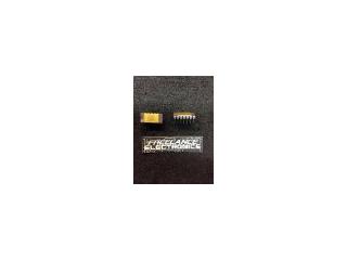
AD5321BRM
Part #
AD5321BRM
Description
IC DAC 12BIT 2.5V 2-WIRE 8-MSOP
Category
IC
Availability
In Stock
Qty
8
Qty
Price
1 - 1
$5.80400
2 - 3
$4.61682
4 - 5
$4.35300
6 - 6
$4.04521
7 +
$3.60552
Manufacturer
Available
Qty
Analog Devices
Freelance Stock:
8
Ships Immediately
Add to Cart
Related Items
Analog Devices
IC
AD5323BRU
$31.09964
Analog Devices
IC
AD5326BRUZ
$12.83297
Analog Devices
IC
AD5326S1
$19.37450
Analog Devices
IC
AD532BRU
$31.79071
Analog Devices
IC
AD532JD
$24.56358
Analog Devices
IC
AD532SE/883B
$112.50510