Freelance Electronics Components Distributor
Closed Dec 25th-26th
800-300-1968
We Stock Hard to Find Parts

74F674N

Part # 74F674N
Description
Category IC
Availability In Stock
Qty 6
Qty Price
1 - 1 $25.66954
2 - 2 $20.41895
3 - 3 $19.25215
4 - 5 $17.89089
6 + $15.94623
Manufacturer Available Qty
Philips Semiconductor
Date Code: 9444
  • Shipping Freelance Stock: 6
    Ships Immediately


Technical Document


DISCLAIMER: The information provided herein is solely for informational purposes. Customers must be aware of the suitability of this product for their application, and consider that variable factors such as Manufacturer, Product Category, Date Codes, Pictures and Descriptions may differ from available inventory.

Philips Semiconductors Product specification
74F67416-bit serial/parallel-in, serial-out shift register (3-State)
1
1989 Feb 05 853–1248 92263
FEATURES
16-bit serial I/O shift register
16-bit parallel-in/serial-out converter
Recirculating serial shifting
Common serial data I/O pin (3-State)
DESCRIPTION
The 74F674 is a 16-bit shift register with serial and parallel load
capability and serial output. A single pin serves alternately as an
input for serial entry or as a 3-State serial output. In the serial out
mode the data recirculates in the register. Chip Select, Read/Write
and Mode inputs provide control flexibility. The 74F674 operates in
one of four modes, as indicated in the Function table.
Hold: A High signal on the Chip Select (CS
) input prevents clocking
and forces the Serial Input/Output (SI/O) 3-State buffer into the high
impedance state.
Serial load: Data present on the SI/O pin shifts into the register on
the falling edge of CP
. Data enters the Q0 position and shifts toward
Q15 on successive clocks.
Serial output: The SI/O 3-State buffer is active and the register
contents are shifted out from Q15 and simultaneously shifted back
into Q0.
Parallel load: Data present on D0–D15 is entered into the register
on the falling edge of CP
. The SI/O 3-State buffer is active and
represents the Q15 output. To prevent false clocking, CP
must be
Low during a Low-to-High transition of CS
.
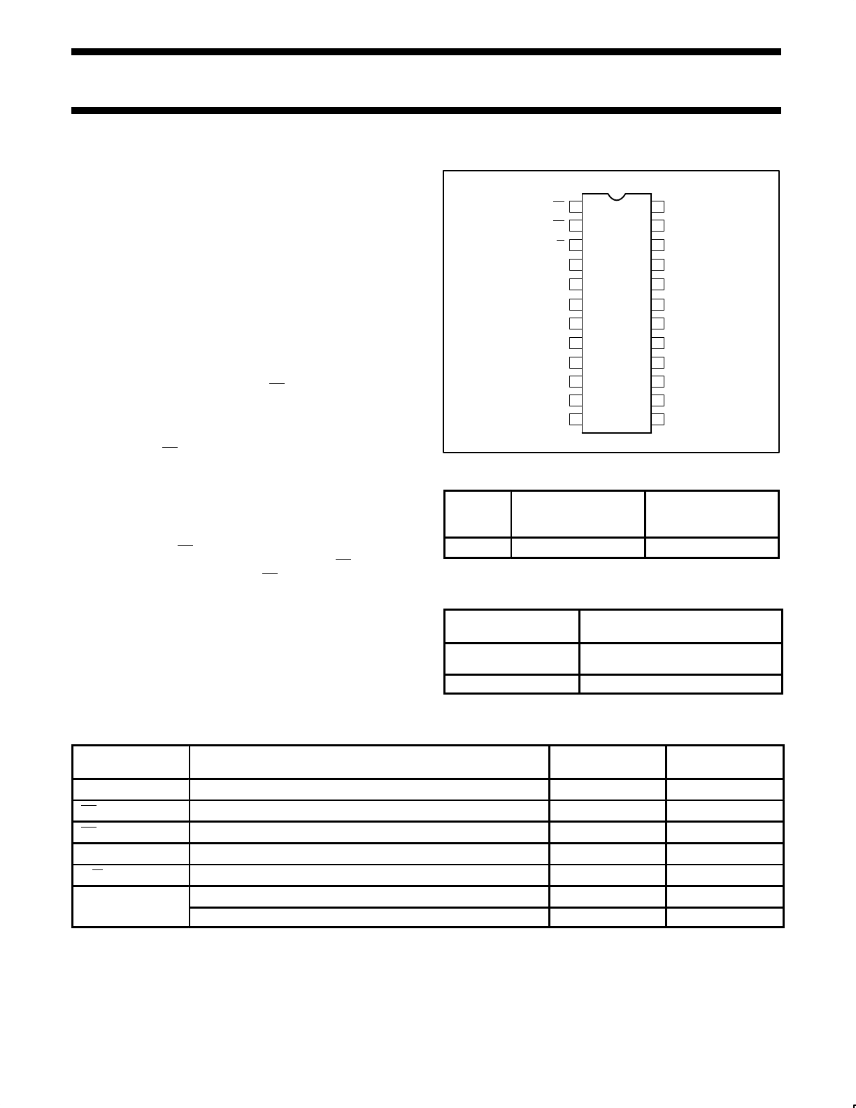
PIN CONFIGURATION
241
V
CC
CS
23
22
21
20
19
18
17
16
10 15
9
8
7
6
5
4
3
2
D15
D14
D11
D10
D9
D8
CP
M
SI/O
D1
D2
D3
D13
D12
NC
R/W
SF01188
D0
D7
14
12 13
11
D6
D4
GND
D5
TYPE TYPICAL f
MAX
TYPICAL SUPPLY
CURRENT
(TOTAL)
74F674 95MHz 55mA
ORDERING INFORMATION
DESCRIPTION COMMERCIAL RANGE
V
CC
= 5V ±10%, T
amb
= 0°C to +70°C
24-Pin Plastic Slim DIP
(300mil)
N74F674N
24-Pin Plastic SOL N74F674D
INPUT AND OUTPUT LOADING AND FAN-OUT TABLE
PINS DESCRIPTION
74F(U.L.)
HIGH/LOW
LOAD VALUE
HIGH/LOW
D0–D15 Parallel data inputs 1.0/1.0 20µA/0.6mA
CS Chip Select input (active Low) 1.0/1.0 20µA/0.6mA
CP Clock Pulse input (active falling edge) 1.0/1.0 20µA/0.6mA
M Mode select input 1.0/1.0 20µA/0.6mA
R/W Read/Write input 1.0/1.0 20µA/0.6mA
SI/O
Serial data input or 3.5/1.0 70mA/0.6mA
SI/O
Serial 3-state output 150/40 3.0mA/24mA
NOTE: One (1.0) FAST Unit Load is defined as: 20µA in the High state and 0.6mA in the Low state.
Philips Semiconductors Product specification
74F67416-bit serial/parallel-in, serial-out shift register (3-State)
1989 Feb 05
2
LOGIC SYMBOL
8910
V
CC
= Pin 24
GND = Pin 12
1
2
SF01189
CP
CS
D0 D1 D4 D5 D6 D7D3D2
11 13 147 16 17 18
D8 D9 D12 D13 D14 D15D11D10
19 20 21 2215 23
3
5
M
R/W
SO
6
FUNCTION TABLE
CONTROL INPUTS
SI/O OPERATING
CS R/W M CP
SI/O
STATUS
OPERATING
MODE
H X X X High Z Hold
L L X Data in Serial load
L H L Data out
Serial output with
recirculation
L H H Active
Parallel load;
no shifting
H = High voltage level
L = Low voltage level
X = Don’t care
= High-to-Low transition of designed input
LOGIC SYMBOL (IEEE/IEC)
SF01190
SRG16
0
1
M
0
3
3, 4D
5
3
1
2
8
9
10
11
13
14
7
16
17
18
19
20
21
22
15
23
3, 4D
3
, 4D
3, 4D
&
&
EN
C4(0/1/2)
6
LOGIC DIAGRAM
V
CC
= Pin 24
GND = Pin 12
SF01191
PE
D0–D15
Q15
CP
Q0
D0–D15 (7–11, 13–23)
5
1
2
3
6
SI/O
M
CS
CP
R/W
Philips Semiconductors Product specification
74F67416-bit serial/parallel-in, serial-out shift register (3-State)
1989 Feb 05
3
ABSOLUTE MAXIMUM RATINGS
(Operation beyond the limits set forth in this table may impair the useful life of the device.
Unless otherwise noted these limits are over the operating free-air temperature range.)
SYMBOL
PARAMETER RATING UNIT
V
CC
Supply voltage –0.5 to +7.0 V
V
IN
Input voltage –0.5 to +7.0 V
I
IN
Input current –30 to +5.0 mA
V
OUT
Voltage applied to output in High output state –0.5 to +V
CC
V
I
OUT
Current applied to output in Low output state 48 mA
T
amb
Operating free-air temperature range 0 to +70 °C
T
stg
Storage temperature –65 to +150 °C
RECOMMENDED OPERATING CONDITIONS
SYMBOL
PARAMETER
LIMITS
UNIT
SYMBOL
PARAMETER
MIN NOM MAX
UNIT
V
CC
Supply voltage 4.5 5.0 5.5 V
V
IH
High-level input voltage 2.0 V
V
IL
Low-level input voltage 0.8 V
I
IK
Input clamp current –18 mA
I
OH
High-level output current –3 mA
I
OL
Low-level output current 24 mA
T
amb
Operating free-air temperature range 0 70 °C
DC ELECTRICAL CHARACTERISTICS
(Over recommended operating free-air temperature range unless otherwise noted.)
SYMBOL
PARAMETER
TEST CONDITIONS
1
LIMITS
UNIT
SYMBOL
PARAMETER
TEST
CONDITIONS
1
MIN TYP
2
MAX
UNIT
V
OH
High-level output voltage
V
CC
= MIN, V
IL
= MAX,
±10%V
CC
2.4 V
V
OH
Hi
g
h
-
l
eve
l
ou
t
pu
t
vo
lt
age
V
CC
MIN, V
IL
MAX,
V
IH
= MIN, I
OH
= MAX
±5%V
CC
2.7 3.3 V
V
OL
Low-level output voltage
V
CC
= MIN, V
IL
= MAX,
±10%V
CC
0.35 0.50 V
V
OL
L
ow-
l
eve
l
ou
t
pu
t
vo
lt
age
V
CC
MIN, V
IL
MAX,
V
IH
= MIN, I
OL
= MAX
±5%V
CC
0.35 0.50 V
V
IK
Input clamp voltage V
CC
= MIN, I
I
= I
IK
–0.73 –1.2 V
I
I
Input current at
SI/O only V
CC
= MAX, V
I
= 5.5V 100 µA
I
I
maximum input voltage
others V
CC
= MAX, V
I
= 7.0V 100 µA
I
IH
High-level input current V
CC
= MAX, V
I
= 2.7V 20 µA
I
IL
Low-level input current V
CC
= MAX, V
I
= 0.5V –0.6 mA
I
OZH
+I
IH
Off-state output current
High-level voltage applied
SI/O
V
CC
= MAX, V
O
= 2.7V 70 µA
I
OZL
+I
IL
Off-state output current
Low-level voltage applied
SI/O
only
V
CC
= MAX, V
O
= 0.5V –600 µA
I
OS
Short-circuit output current
3
V
CC
= MAX –60 –150 mA
I
CC
Supply current (total) V
CC
= MAX 55 80 mA
NOTES:
1. For conditions shown as MIN or MAX, use the appropriate value under the recommended operating conditions for the applicable type.
2. All typical values are at V
CC
= 5V, T
amb
= 25°C.
3. Not more than one output should be shorted at a time. For testing I
OS
, the use of high-speed test apparatus and/or sample-and-hold
techniques are preferable in order to minimize internal heating and more accurately reflect operational values. Otherwise, prolonged shorting
of a High output may raise the chip temperature well above normal and thereby cause invalid readings in other parameter tests. In any
sequence of parameter tests, I
OS
should be performed last.
12NEXT