Closed Dec 25th-26th
800-300-1968
We Stock Hard to Find Parts
My Account
|
My Orders
|
My Cart
Questions?
(800) 300-1968
Register
(current)
My Account
(current)
My Orders
(current)
My Cart
(current)
Categories
(current)
Manufacturers
Request a Quote
Sell Your Excess
Consignment
Quality Assurance
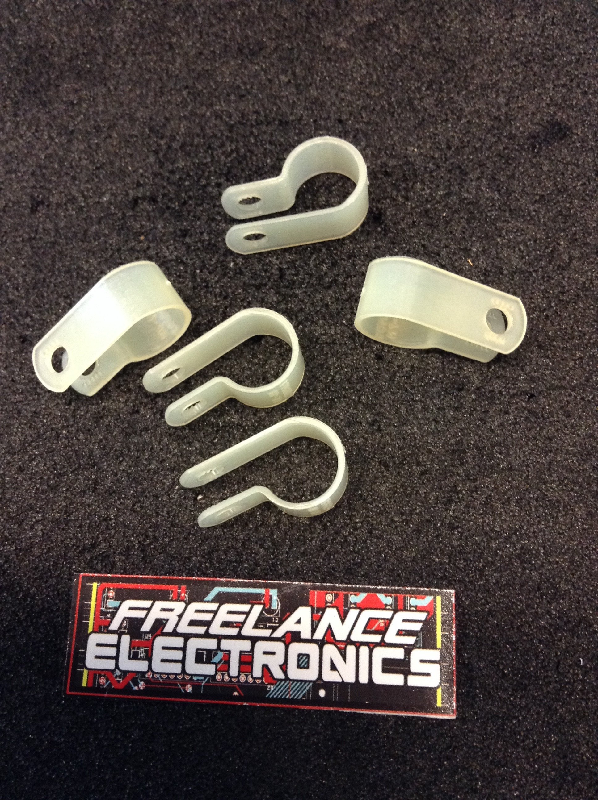
HP-7N
Part #
HP-7N
Description
CBL ACC CBL HANGER NYLON WHITE/BLK - Bulk
Category
HARDWARE
Availability
In Stock
Qty
33
Qty
Price
1 +
$0.14506
Manufacturer
Available
Qty
BURNDY CORP
Freelance Stock:
33
Ships Immediately
Add to Cart
Related Items
ANTENNA PRODUCTS
HARDWARE
0002-1389-201
$15.36322
Airlab
HARDWARE
00140720011
$5.07754
PILOT
HARDWARE
00724-18-00341-001
GILBERT ENGINEERING
HARDWARE
0119-774-3
Military Spec
HARDWARE
0134-CLP-0001
Generic
HARDWARE
0148085