Freelance Electronics Components Distributor
Closed Dec 25th-26th
800-300-1968
We Stock Hard to Find Parts

C1925

Part # C1925
Description BLOCK, JUNCTION - Bulk
Category HARDWARE
Availability In Stock
Qty 2
Qty Price
1 + $24.92401
Manufacturer Available Qty
MAGNUM
  • Shipping Freelance Stock: 2
    Ships Immediately


Technical Document


DISCLAIMER: The information provided herein is solely for informational purposes. Customers must be aware of the suitability of this product for their application, and consider that variable factors such as Manufacturer, Product Category, Date Codes, Pictures and Descriptions may differ from available inventory.

Hardware Description
AVR STK500 User Guide 3-21
1925C–AVR–3/03
When the XTAL1 jumper is mounted, the STK500 internal clock system is used as main
clock to the target AVR. The internal clock system can either use a crystal in the
on-board crystal socket or a software-generated clock from the master microcontroller.
The frequency of the software-generated clock can be set from 0 to 3.68 MHz. The
default value is 3.68 MHz. Section 5.3.5.3 on page 5-7 explains how to set the clock fre-
quency from AVR Studio.
When using the STK500 software-generated clock system as main clock, the target
AVR microcontroller fuses should be configured for “external clock” as clock source.
This gives shortest start-up time for the microcontroller. For details of start-up time, see
the datasheet for the AVR microcontroller. For an explanation of clock source fuses con-
figuration, see Section 5.3.2 on page 5-3. Not all AVR devices have fuses for selection
between using a crystal or oscillator as clock source.
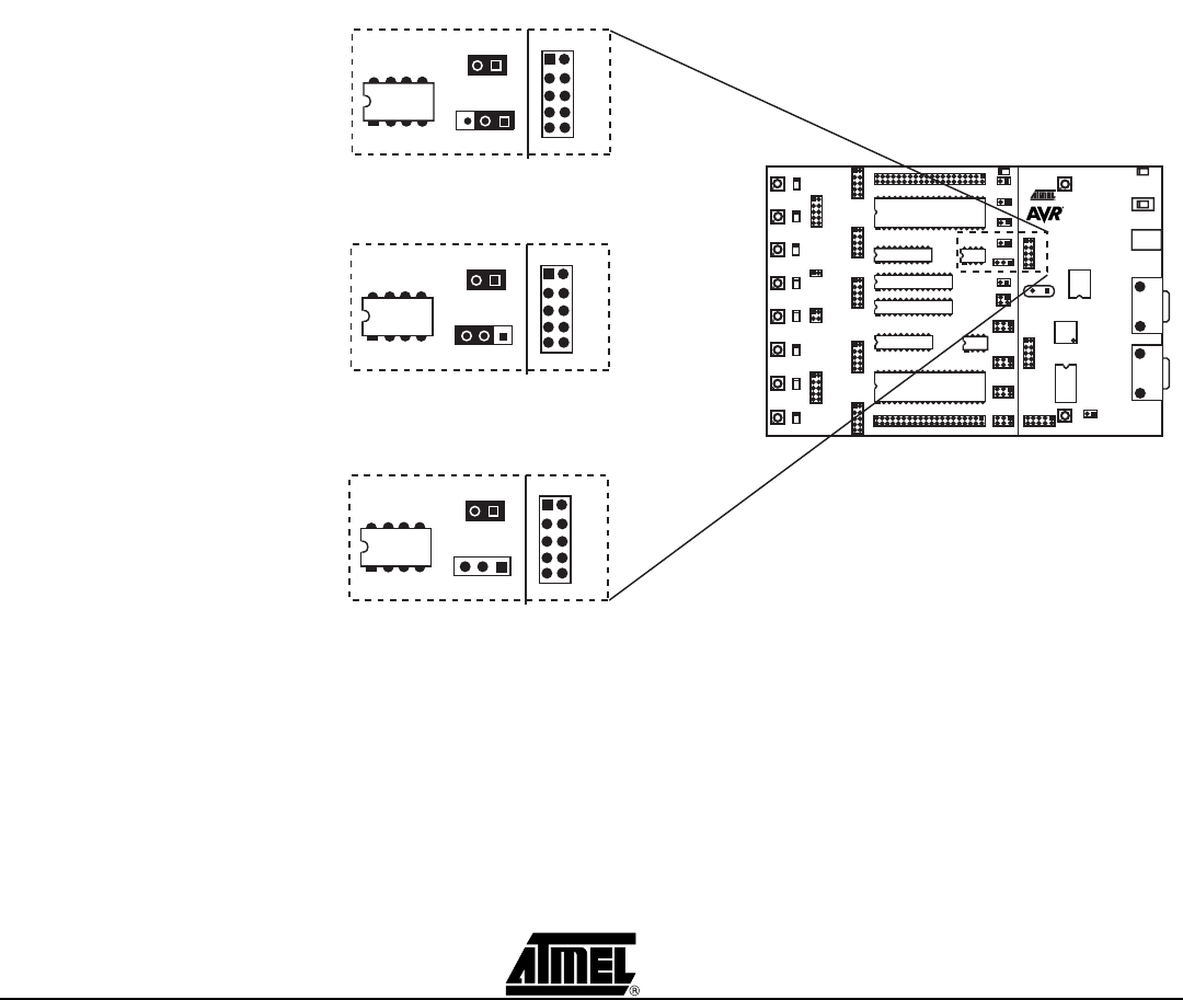
The internal clock system is selected with the OSCSEL jumper. Figure 3-29 shows the
jumper options for OSCSEL.
The on-board oscillator will work with ceramic resonators or crystals between
2 - 20 MHz (AT-cut, fundamental and parallel resonant crystals).
Figure 3-29. OSCSEL Jumper Options
When programming AVR in High-voltage Programming mode, OSCSEL should be
mounted on pins 1 and 2 to give the master microcontroller control of the target clock.
This is explained in detail in Section 3.7.2 on page 3-11.
Note: In a real application with only one AVR connected to the crystal, there is no
need for an external oscillator circuit. The STK500 has eight different AVR
sockets connected to the same clock system. The long signal lines in this
system makes it difficult to drive a crystal with the On-chip Oscillators on the
AVR. The oscillator on STK500 is designed to operate on all target voltages
from 1.8 to 6.0V.
XTAL1
OSCSEL
Jumper mounted on pins 1 and 2
On-board software clock signal connected (default)
Jumper mounted on pins 2 and 3
On-board crystal signal connected
Jumper not mounted
On-board XTAL1 signal disconnected
XTAL1
OSCSEL
XTAL1
OSCSEL
Hardware Description
3-22 AVR STK500 User Guide
1925C–AVR–3/03
Figure 3-30. XTAL1 and OSCSEL Connections
3.8.5 BSEL2 Jumper The BSEL2 jumper connects the Byte Select 2 signal for High-voltage Programming of
ATmega8, ATmega16, ATmega161, ATmega163, ATmega128, and ATmega323. The
BSEL2 jumper should only be mounted when High-voltage Programming ATmega16,
ATmega161, ATmega163, ATmega128, or ATmega323. When using ATmega8, con-
nect the right BSEL2 pin to PC2 in the target area. See Figure 3-31. For descriptions of
the Byte Select 2 signal, see the programming section of the corresponding parts
datasheet.
Figure 3-31. BSEL2 Connection for ATmega8
3.8.6 PJUMP Jumpers The PJUMP jumpers route the programming pin of AT90S2333, AT90S4433, and
ATmega8 to the programming lines when using High-voltage Programming. The
PJUMP jumpers should only be mounted when using High-voltage Programming on
AT90S2333, AT90S4433, or ATmega8. During debugging, High-voltage Programming
of other parts and ISP programming, these jumpers should not be mounted.
Figure 3-32. PJUMP Jumpers Placement
PE1
RST
GND
XT2
VTG
PE0
PE2
REF
XT1
GND
1 2
XTAL1 NET
XTAL1
Voltage
converter
VTG5V
AVR
Studio
MASTER
MCU
CRYSTAL
PORTE
Jumper
Jumper
Oscillator
OSCSEL
3
2
1
BSEL2
PJUMP
Cable to PC2
Correct
Jumper
Placement
Not
Correct
Hardware Description
AVR STK500 User Guide 3-23
1925C–AVR–3/03
3.9 Expansion
Connectors
STK500 has two expansion connectors, one on each side of the programming module.
All AVR I/O ports, programming signals and control signals are routed to the expansion
connectors. The expansion connectors allow easy prototyping of applications
with STK500. The pinout of the expansion connectors is shown in Figure 3-34 and Fig-
ure 3-35.
Figure 3-33. Expansion Headers
Expansion Header 0
Expansion Header 1
Prog Ctrl
Prog Data
Pin 1
Pin 1
PREVIOUS4567891011121314151617NEXT