Closed Dec 25th-26th
800-300-1968
We Stock Hard to Find Parts
My Account
|
My Orders
|
My Cart
Questions?
(800) 300-1968
Register
(current)
My Account
(current)
My Orders
(current)
My Cart
(current)
Categories
(current)
Manufacturers
Request a Quote
Sell Your Excess
Consignment
Quality Assurance
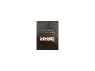
1N5415
Part #
1N5415
Description
Diode Switching 50V 3A 2-PinCase E - Bulk
Category
DIODE
Availability
Out of Stock
Qty
0
Qty
Price
1 +
$1.16470
Related Items
Military Spec
DIODE
1N5416
$1.36979
Microsemi Corp
DIODE
1N5417
$0.35139
Microsemi Corp
DIODE
1N5417US
$5.11782
General Instrument
DIODE
1N5418
$6.17895
Military Spec
DIODE
0027594835-01
OPTO ELECTRONICS
DIODE
0125
$20.09019