Closed Dec 25th-26th
800-300-1968
We Stock Hard to Find Parts
My Account
|
My Orders
|
My Cart
Questions?
(800) 300-1968
Register
(current)
My Account
(current)
My Orders
(current)
My Cart
(current)
Categories
(current)
Manufacturers
Request a Quote
Sell Your Excess
Consignment
Quality Assurance
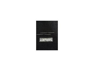
1N5338B
Part #
1N5338B
Description
DIODE ZENER 5.1V 5W AXIAL
Category
DIODE
Availability
Out of Stock
Qty
0
Qty
Price
1 +
$1.52756
Related Items
NEW JERSEY SEMI
DIODE
1N5333
$9.42760
Motorola Corp
DIODE
1N5333B
$0.20552
Microsemi Corp
DIODE
1N5335C
$4.92194
Military Spec
DIODE
1N5336
$3.69660
ON Semiconductor
DIODE
1N5336BRLG
$0.06861
Motorola Corp
DIODE
1N5337B
$0.15401