Closed Dec 25th-26th
800-300-1968
We Stock Hard to Find Parts
My Account
|
My Orders
|
My Cart
Questions?
(800) 300-1968
Register
(current)
My Account
(current)
My Orders
(current)
My Cart
(current)
Categories
(current)
Manufacturers
Request a Quote
Sell Your Excess
Consignment
Quality Assurance
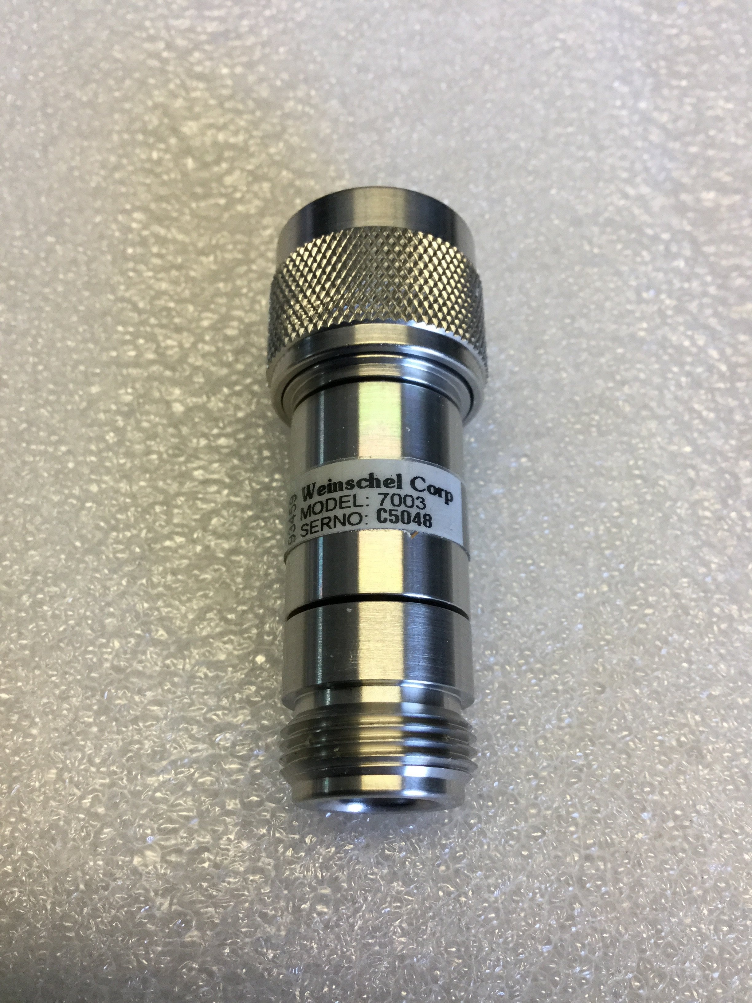
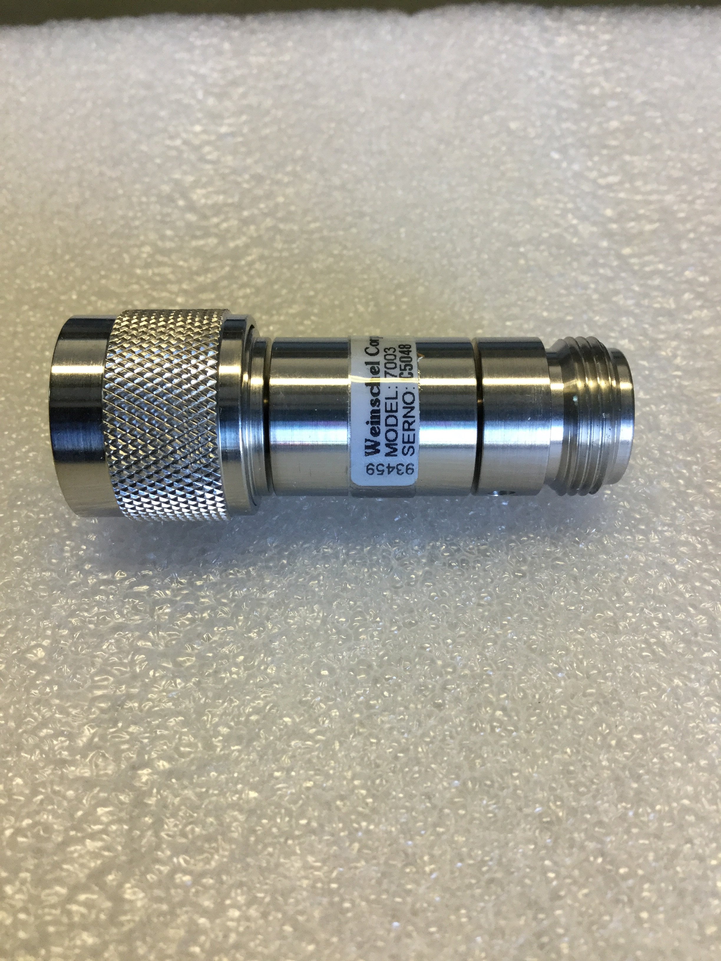
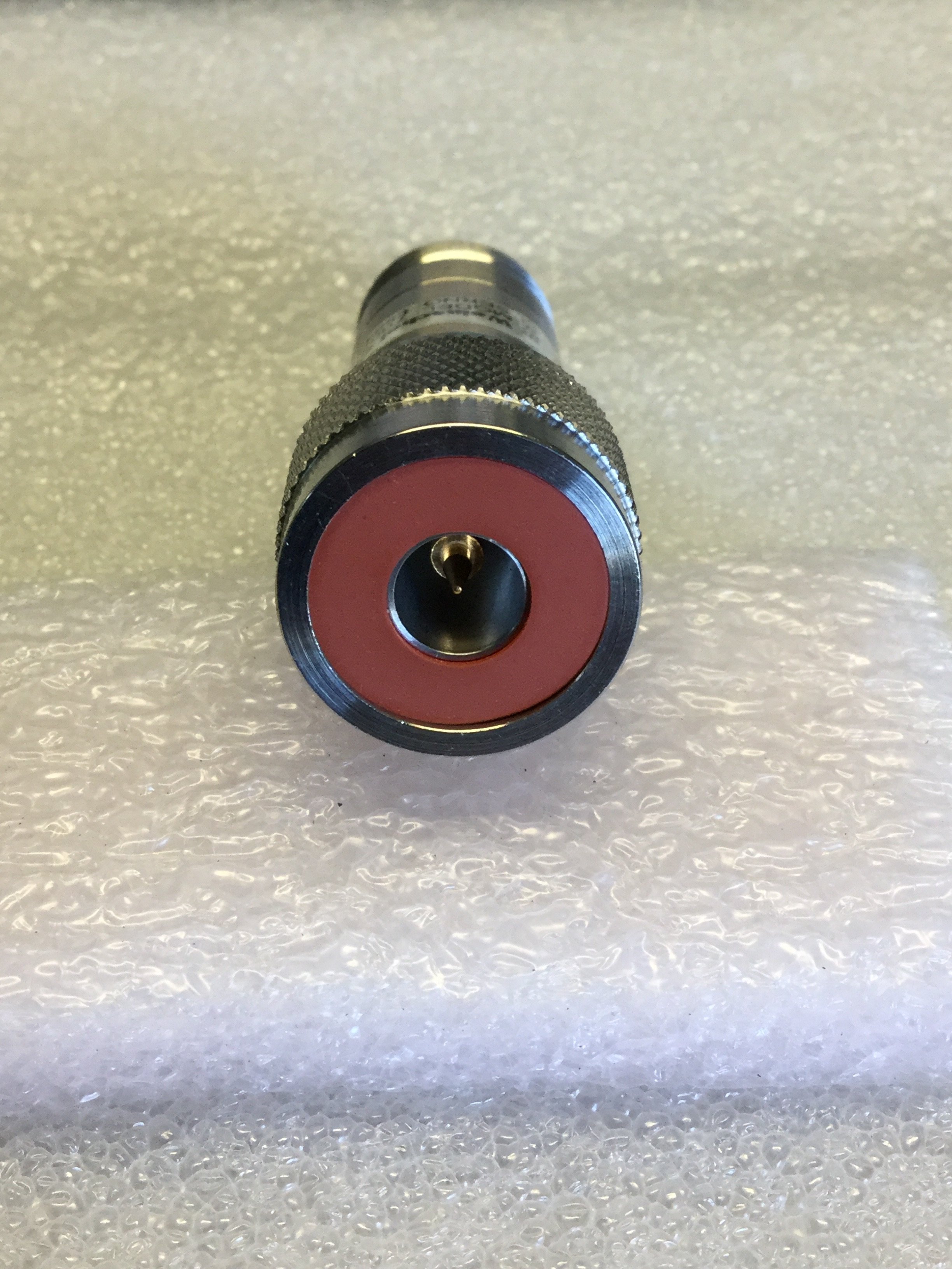
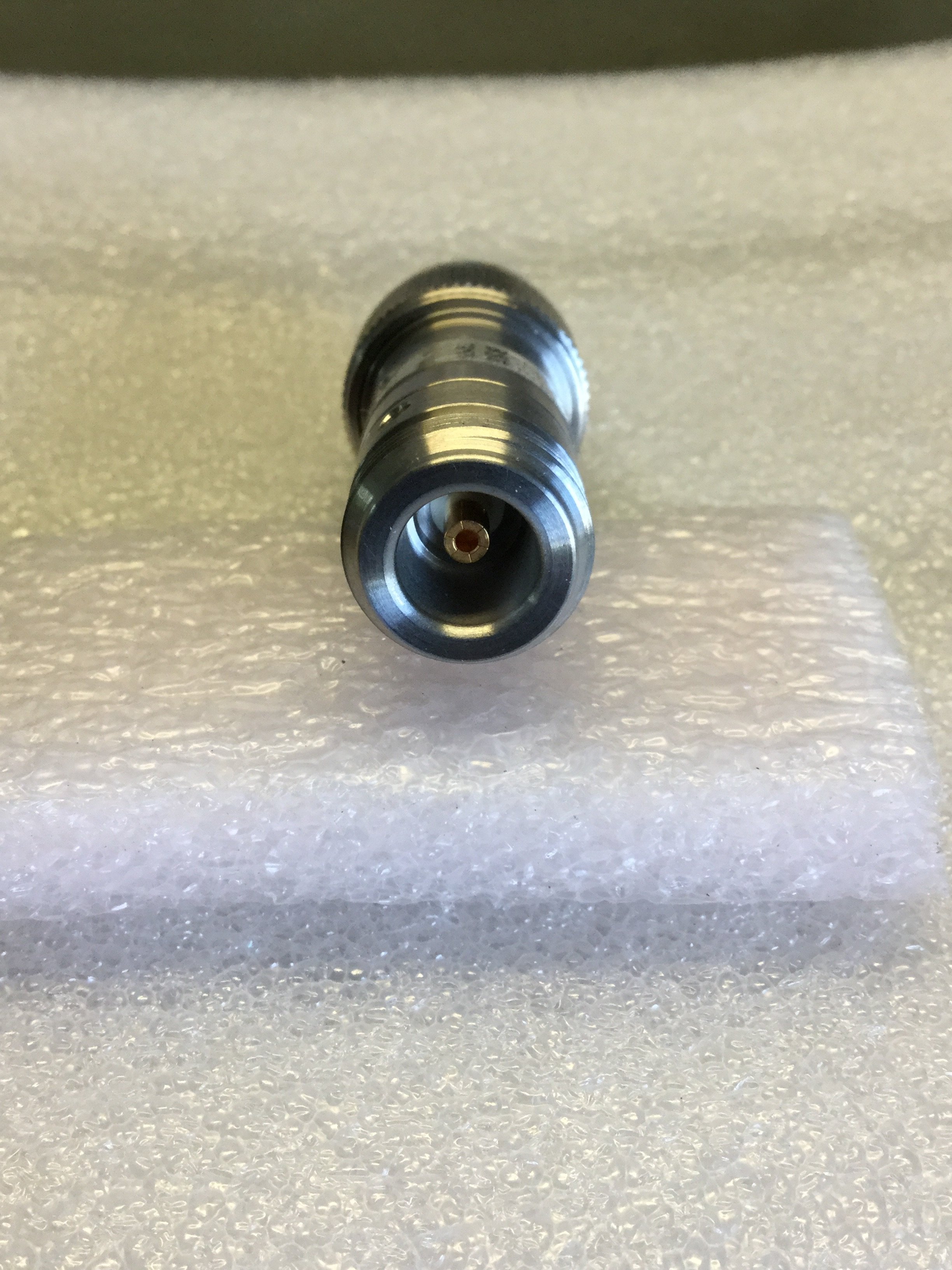
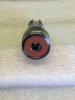
7003
Part #
7003
Description
DC Blocks 9kHz to 18.3 GHzN Connector
Category
CONNECTOR
Availability
In Stock
Qty
15
Qty
Price
1 - 1
$112.50510
2 - 3
$89.49270
4 - 6
$84.37883
7 - 9
$78.41265
10 +
$69.88953
Manufacturer
Available
Qty
WEINSCHEL CORP
Freelance Stock:
15
Ships Immediately
Add to Cart
Related Items
WEINSCHEL CORP
CONNECTOR
7003
$112.50510
AMP
CONNECTOR
0-0176763-1
$2.40963
AMP
CONNECTOR
0-0822475-2
$2.00801
AMP
CONNECTOR
0-0925486-1
$1.83223
KYOCERA
CONNECTOR
00-6200-506-130-000+
$0.45646
ELCO CORP.
CONNECTOR
00-7008-047-163-100
$20.75398