Freelance Electronics Components Distributor
Closed Dec 25th-26th
800-300-1968
We Stock Hard to Find Parts

06032U1R5BAT2A

Part # 06032U1R5BAT2A
Description CAP 1.5PF 200VDC C0G 0.1PF SMD 0603 - Tape and Reel
Additional Information:


Category CAPACITOR
Availability In Stock
Qty 4000
Qty Price
1 - 840 $0.05295
841 - 1,680 $0.04212
1,681 - 2,520 $0.03971
2,521 - 3,360 $0.03690
3,361 + $0.03289
Manufacturer Available Qty
AVX CORPORATION
Date Code: 0926
  • Shipping Freelance Stock: 4000
    Ships Immediately


Technical Document


DISCLAIMER: The information provided herein is solely for informational purposes. Customers must be aware of the suitability of this product for their application, and consider that variable factors such as Manufacturer, Product Category, Date Codes, Pictures and Descriptions may differ from available inventory.

TQP7M9102
½W High Linearity Amplifier
Typical Performance 2110-2170 MHz
Frequency MHz 2110 2140 2170
Gain dB 17.9 17.8 17.7
Input Return Loss dB -12 -12 -11
Output Return Loss dB -12 -11 -10
Output P1dB dBm +27.8 +27.6 +27.4
Output IP3 (+9 dBm/tone, f = 1 MHz)
dBm +43.6 +43.5 +43.6
WCDMA Channel Power (at -50 dBc ACLR) [1] dBm +18.5 +18.4 +18.3
Noise Figure dB 3.8
Notes:
1. ACLR Test set-up: 3GPP WCDMA, TM1+64 DPCH, +5 MHz offset, PAR = 10.2 dB at 0.01% Prob.
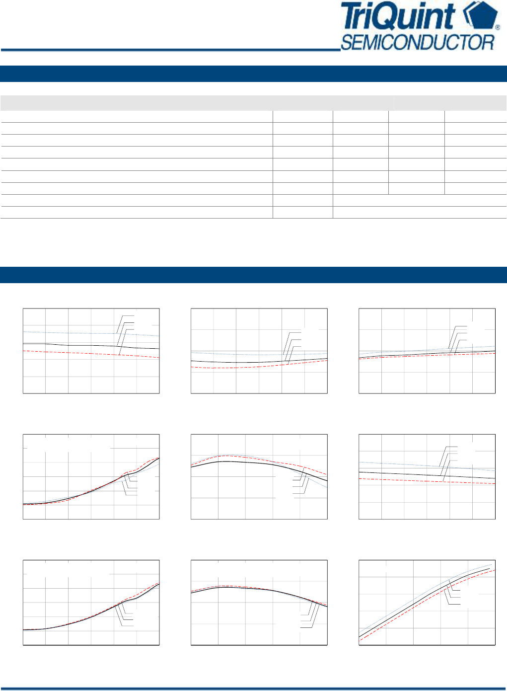
RF Performance Plots 2110-2170 MHz
15
16
17
18
19
20
2110 2120 2130 2140 2150 2160 2170
Gain (dB)
Freq (MHz)
Gain vs. Frequency
40
°
C
+25
°
C
3.9 4.0
Supply Voltage, Vcc V 5
Quiescent Collector Current, Icq mA 137
-20
-15
-10
-5
0
2110 2120 2130 2140 2150 2160 2170
Retun Loss (dB)
Freq (MHz)
Input Return Loss vs. Frequency
40
°
C
+25
°
C
-20
-15
-10
-5
0
2110 2120 2130 2140 2150 2160 2170
Retun Loss (dB)
Freq (MHz)
Output Return Loss vs. Frequency
40
°
C
+25
°
C
+8
5
°
C
+8
5
°
C
+85
°
C
-65
-60
-55
-50
-45
-40
-35
14 15 16 17 18 19 20
ACLR (dBc)
Pout (dBm)
ACLR Vs. Output Power
38
40
42
44
46
7 9 11 13 15 17
OIP3 (dBm)
Pout/Tone (dBm)
OIP3 Vs. Pout/Tone
25
26
27
28
29
30
2110 2120 2130 2140 2150 2160 2170
P1dB (dBm)
Frequency (MHz)
P1dB vs. Frequency
40
°
C
+25
°
C
W-CDMA 3GPP Test Model 1+64 DPCH
PAR = 10.2 dB @ 0.01% Probability
3.84 MHz BW
Data Sheet: Rev D 10/04/11
- 6 of 9 -
Disclaimer: Subject to change without notice
© 2011 TriQuint Semiconductor, Inc.
Connecting the Digital World to the Global Network
®
+85
°
C
+25
°
C
40
°
C
Freq.= 2140 MHz
+85
°
C
+25
°
C
40
°
C
Freq.=2140 MHz
1 MHz Tone Spacing
+8
5
°
C
-65
-60
-55
-50
-45
-40
-35
14 15 16 17 18 19 20
ACLR (dBc)
Pout (dBm)
ACLR Vs. Output Power
38
40
42
44
46
7 9 11 13 15 17
OIP3 (dBm)
Pout/Tone (dBm)
OIP3 Vs. Pout/Tone
2170 MHz
2140 MHz
2110 MHz
W-CDMA 3GPP Test Model 1+64 DPCH
PAR = 10.2 dB @ 0.01% Probability
3.84 MHz BW
Temp.=+25
°
C
2170 MHz
2140 MHz
2110 MHz
W-CDMA 3GPP Test Model 1+64 DPCH
PAR = 10.2 dB @ 0.01% Probability
3.84 MHz BW
1 MHz Tone Spacing
Te
mp.=+25
°
C
19
21
23
25
27
29
2468101
Pout (dBm)
Pin (dBm)
Output Power vs. Input Power
2
Freq.=2140 MHz
40
°
C
+25
°
C
+8
5
°
C
TQP7M9102
½W High Linearity Amplifier
Pin Configuration and Description
RF IN GND RF OUT
GND
1
23
4
Pin Symbol Description
1 RF IN
RF Input. Requires external match for optimal performance. External DC Block
required.
2, 4 GND RF/DC Ground Connection
3 RFout / Vcc
RF Output. Requires external match for optimal performance. External DC Block
and supply voltage is required.
Applications Information
PC Board Layout
Data Sheet: Rev D 10/04/11
- 7 of 9 -
Disclaimer: Subject to change without notice
© 2011 TriQuint Semiconductor, Inc.
Connecting the Digital World to the Global Network
®
PCB Material (stackup):
1071363AW REV - 1071363PC REV -
GND
+V
CC
SOT89 EVAL. BRD., 1/2 WATT
1 oz. Cu top layer
0.014 inch Nelco N-4000-13, ε
r
=3.7
1 oz. Cu MIDDLE layer 1
Core Nelco N-4000-13
1 oz. Cu middle layer 2
0.014 inch Nelco N-4000-13
1 oz. Cu bottom layer
Finished board thickness is 0.062±.006
50 ohm line dimensions: width = .031”, spacing = .035”.
The pad pattern shown has been developed and tested for
optimized assembly at TriQuint Semiconductor. The PCB
land pattern has been developed to accommodate lead and
package tolerances. Since surface mount processes vary
from supplier to supplier, careful process development is
recommended.
TQP7M9102
½W High Linearity Amplifier
Mechanical Information
Package Information and Dimensions
This package is lead-free/RoHS-
compliant. The plating material on the
leads is NiPdAu. It is compatible with
both lead-free (maximum 260 °C reflow
temperature) and lead (maximum 245 °C
reflow temperature) soldering processes.
Data Sheet: Rev D 10/04/11
- 8 of 9 -
Disclaimer: Subject to change without notice
© 2011 TriQuint Semiconductor, Inc.
Connecting the Digital World to the Global Network
®
Th
e component will be marked with a
“7M9102” designator with an
alphanumeric lot code on the top surface
of package.
7M9102
Mounting Configuration
All dimensions are in millimeters (inches). Angles are in degrees.
Notes:
1. Ground / thermal vias are critical for the proper performance of this device. Vias should use a .35mm (#80 / .0135”) diameter drill and
have a final plated thru diameter of .25 mm (.010”).
2. Add as much copper as possible to inner and outer layers near the part to ensure optimal thermal performance.
3. RF trace width depends upon the PC board material and construction.
4. Use 1 oz. Copper minimum.
PREVIOUS1234567NEXT