Freelance Electronics Components Distributor
Closed Dec 25th-26th
800-300-1968
We Stock Hard to Find Parts

06032U1R5BAT2A

Part # 06032U1R5BAT2A
Description CAP 1.5PF 200VDC C0G 0.1PF SMD 0603 - Tape and Reel
Additional Information:


Category CAPACITOR
Availability In Stock
Qty 4000
Qty Price
1 - 840 $0.05295
841 - 1,680 $0.04212
1,681 - 2,520 $0.03971
2,521 - 3,360 $0.03690
3,361 + $0.03289
Manufacturer Available Qty
AVX CORPORATION
Date Code: 0926
  • Shipping Freelance Stock: 4000
    Ships Immediately


Technical Document


DISCLAIMER: The information provided herein is solely for informational purposes. Customers must be aware of the suitability of this product for their application, and consider that variable factors such as Manufacturer, Product Category, Date Codes, Pictures and Descriptions may differ from available inventory.

TQP7M9102
½W High Linearity Amplifier
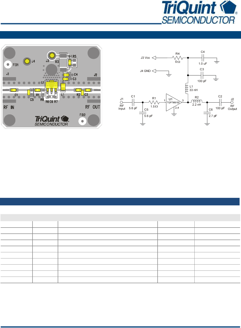
Application Circuit 869-960 MHz (TQP7M9102-PCB900)
1071363AW REV - 1071363PC REV -
GND
+VCC
SOT89 EVAL. BRD., 1/2 WATT
L1
C1
U1
R1
C5
C2
C3
C4
R4
J3
J4
R2
C6
Data Sheet: Rev D 10/04/11
- 3 of 9 -
Disclaimer: Subject to change without notice
© 2011 TriQuint Semiconductor, Inc.
Connecting the Digital World to the Global Network
®
N
otes:
1. See PC Board Layout, page 7 for more information.
2. Components shown on the silkscreen but not on the schematic are not used.
3. 0 resistor (R4) may be replaced with copper trace in the target application layout.
4. The recommended component values are dependent upon the frequency of operation.
5. All components are of 0603 size unless stated on the schematic.
6. Critical component placement locations:
Distance from U1 Pin 1 (left edge) to C5 (right edge): 255 mils (12.1 deg. at 920 MHz)
Distance from U1 Pin 1 (left edge) to C1 (right edge): 460 mils (21.9 deg. at 920 MHz)
Distance from U1 Pin 3 (right edge) to R2 (left edge): 290 mils (13.8 deg. at 920 MHz)
Distance from U1 Pin 3 (right edge) to C6 (left edge): 370 mils (17.6 deg. at 920 MHz)
Bill of Material
Ref Des Value Description Manuf. Part Number
n/a n/a Printed Circuit Board
TriQuint 1071363
U1 n/a TQP7M9102 Amplifier, SOT-89 pkg.
TriQuint TQP7M9102
R4 0 Resistor, Chip, 0603, 5%, 1/16W
various
R1 1.5 Resistor, Chip, 0603, 5%, 1/16W
various
R2 2.2 nH Inductor, 0603, +/-0.3 nH
Toko LL1608-FSL2N2S
L1 33 nH Inductor, 0805, 5%, Coilcraft CS Series
Coilcraft 0805CS-330XJLB
C1, C5 5.6 pF Cap., Chip, 0603, +/-0.1pF. 200V. NPO/COG
AVX 06032U5R6BAT2A
C6 2.7 pF Cap., Chip, 0603, +/-0.1pF. 200V. NPO/COG
AVX 06032U2R7BAT2A
C2, C3
100 pF Cap., Chip, 5%, 50V, NPO/COG
various
C4 1.0 uF Cap., Chip, 10%, 10V, X5R
various
TQP7M9102
½W High Linearity Amplifier
Typical Performance 869-960 MHz
Frequency MHz 869 920 960
Gain dB 21.8 21.9 21.7
Input Return Loss dB -10 -16 -17
Notes:
1. ACLR Test set-up: 3GPP WCDMA, TM1+64 DPCH, +5 MHz offset, PAR = 10.2 dB at 0.01% Prob.
Output Return Loss dB -12 -10 -9
Output P1dB dBm +27.3 +27.4 +27.4
Output IP3 (+19 dBm/tone, f = 1 MHz)
dBm +42.7 +43.4 +43.9
WCDMA Channel Power (at -50 dBc ACLR) [1] dBm +18.0 +18.2 +18.1
Noise Figure dB 5.9 5.9 5.9
Supply Voltage, Vcc V +5
Quiescent Collector Current, Icq mA 137
RF Performance Plots 869-960 MHz
19
20
21
22
23
24
860 880 900 920 940 960
Gain (dB)
Freq (MHz)
Gain vs. Frequency
40
°
C
+25
°
C
-25
-20
-15
-10
-5
0
860 880 900 920 940 960
Return Loss (dB)
Freq (MHz)
Input Return Loss vs. Frequency
40
°
C
+25
°
C
-25
-20
-15
-10
-5
0
86088090092094096
Return Loss (dB)
Freq (MHz)
Output Return Loss vs. Frequency
0
40
°
C
+25
°
C
+8
5
°
C
+8
5
°
C
+8
5
°
C
-65
-60
-55
-50
-45
-40
-35
12 13 14 15 16 17 18 19 20
ACLR (dBc)
Pout (dBm)
ACLR Vs. Output Power
36
38
40
42
44
46
11 13 15 17 19 21
OIP3 (dBm)
Pout/Tone (dBm)
OIP3 Vs. Pout/Tone
25
26
27
28
29
30
86088090092094096
P1dB (dBm)
Frequency (MHz)
P1dB vs. Frequency
Freq.=920 MHz
1 MHz Tone Spacing
Data Sheet: Rev D 10/04/11
- 4 of 9 -
Disclaimer: Subject to change without notice
© 2011 TriQuint Semiconductor, Inc.
Connecting the Digital World to the Global Network
®
+85
°
C
+25
°
C
40
°
C
W-CDMA 3GPP Test Model 1+64 DPCH
PAR = 10.2 dB @ 0.01% Probability
3.84 MHz BW
Freq.=920 MHz
0
40
°
C
+25
°
C
+8
5
°
C
+85
°
C
+25
°
C
40
°
C
-65
-60
-55
-50
-45
-40
-35
12 13 14 15 16 17 18 19 20
ACLR (dBc)
Pout (dBm)
ACLR Vs. Output Power
36
38
40
42
44
46
11 13 15 17 19 21
OIP3 (dBm)
Pout/Tone (dBm)
OIP3 Vs. Pout/Tone
960 MHz
920 MHz
869 MHz
W-CDMA 3GPP Test Model 1+64 DPCH
PAR = 10.2 dB @ 0.01% Probability
3.84 MHz BW
Temp.=+25
°
C
960 MHz
920 MHz
869 MHz
19
21
23
25
27
29
-3 -1 1 3 5 7
Pout (dBm)
Pin (dBm)
Output Power vs. Input Power
40
°
C
+25
°
C
1 MHz Tone Spacing
Temp.=+25
°
C
Freq.= 920 MHz
+8
5
°
C
TQP7M9102
½W High Linearity Amplifier
Application Circuit 2110-2170 MHz (TQP7M9102-PCB2140)
1071363AW REV - 1071363PC REV -
GND
+VCC
SOT89 EVAL. BRD., 1/2 WATT
L1
R8
C6
R4
Data Sheet: Rev D 10/04/11
- 5 of 9 -
Disclaimer: Subject to change without notice
© 2011 TriQuint Semiconductor, Inc.
Connecting the Digital World to the Global Network
®
Bill of Material
Ref Des Value Description Manuf. Part Number
n/a n/a Printed Circuit Board TriQuint 1071363
U1 n/a TQP7M9102 Amplifier, SOT-89 pkg. TriQuint TQP7M9102
C1, R2, R4 0 Resistor, Chip, 0603, 5%, 1/16W various
L1 18 nH Inductor, 0805, Coilcraft CS Series Coilcraft 0805CS-180XJLB
R1, R8 1.5 pF Cap., Chip, 0603, +/-0.1pF. 200V. NPO/COG AVX 06032U1R5BAT2A
C2 3.3 pF Cap., Chip, 0603, +/-0.1pF. 200V NPO/COG AVX 06032U3R3BAT2A
C3 22 pF Cap., Chip, 5%, 50V, NPO/COG various
C4 1.0 uF Cap., Chip, 10%, 10V, X5R various
C6 0.8 pF Cap., Chip, 0603, +/-0.1pF. 200V NPO/COG AVX 06032U0R8BAT2A
N
otes:
1. See PC Board Layout, page 7 for more information.
2. Components shown on the silkscreen but not on the schematic are not used.
3. 0 resistors (C1, R2) may be replaced with copper trace in the target application layout.
4. The recommended component values are dependent upon the frequency of operation.
5. All components are of 0603 size unless stated on the schematic.
6. Critical component placement locations:
Distance from U1 Pin 1 (left edge) to R8 (right edge): 40 mils (4.4 deg. at 2140 MHz)
Distance from U1 Pin 1 (left edge) to R1 (right edge): 115 mils (12.7 deg. at 2140 MHz)
Distance from U1 Pin 3 (right edge) to C6 (left edge): 180 mils (19.9 deg. at 2140 MHz)
Distance from U1 Pin 3 (right edge) to C2 (left edge): 450 mils (49.8 deg. at 2140 MHz)
PREVIOUS1234567NEXT