SCDS017M − MAY 1995 − REVISED JANUARY 2004
3
POST OFFICE BOX 655303 • DALLAS, TEXAS 75265
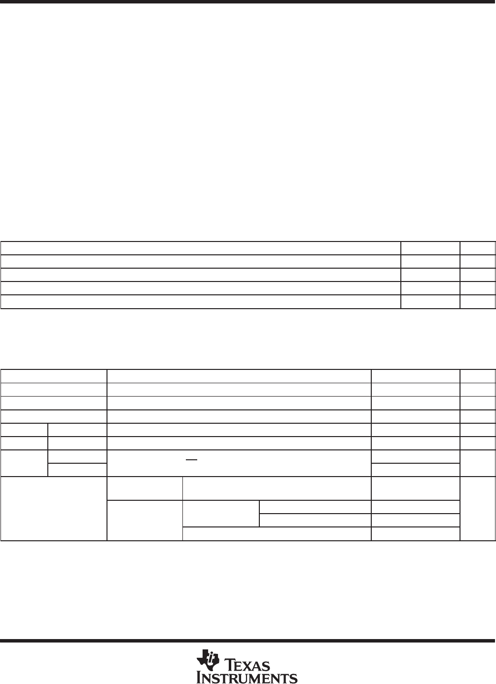
absolute maximum ratings over operating free-air temperature range (unless otherwise noted)
†
Supply voltage range, V
CC
−0.5 V to 7 V. . . . . . . . . . . . . . . . . . . . . . . . . . . . . . . . . . . . . . . . . . . . . . . . . . . . . . . . . .
Input voltage range, V
I
(see Note 1) −0.5 V to 7 V. . . . . . . . . . . . . . . . . . . . . . . . . . . . . . . . . . . . . . . . . . . . . . . . . .
Continuous channel current 128 mA. . . . . . . . . . . . . . . . . . . . . . . . . . . . . . . . . . . . . . . . . . . . . . . . . . . . . . . . . . . . . .
Input clamp current, I
K
(V
I/O
< 0) −50 mA. . . . . . . . . . . . . . . . . . . . . . . . . . . . . . . . . . . . . . . . . . . . . . . . . . . . . . . . . .
Package thermal impedance, θ
JA
(see Note 2): D package 73°C/W. . . . . . . . . . . . . . . . . . . . . . . . . . . . . . . . . . .
(see Note 2): DB package 82°C/W. . . . . . . . . . . . . . . . . . . . . . . . . . . . . . . . .
(see Note 2): DBQ package 90°C/W. . . . . . . . . . . . . . . . . . . . . . . . . . . . . . . .
(see Note 2): PW package 108°C/W. . . . . . . . . . . . . . . . . . . . . . . . . . . . . . . .
(see Note 3): RGY package 39°C/W. . . . . . . . . . . . . . . . . . . . . . . . . . . . . . . .
Storage temperature range, T
stg
−65°C to 150°C. . . . . . . . . . . . . . . . . . . . . . . . . . . . . . . . . . . . . . . . . . . . . . . . . . .
†
Stresses beyond those listed under “absolute maximum ratings” may cause permanent damage to the device. These are stress ratings only, and
functional operation of the device at these or any other conditions beyond those indicated under “recommended operating conditions” is not
implied. Exposure to absolute-maximum-rated conditions for extended periods may affect device reliability.
NOTES: 1. The input and output negative-voltage ratings may be exceeded if the input and output clamp-current ratings are observed.
2. The package thermal impedance is calculated in accordance with JESD 51-7.
3. The package thermal impedance is calculated in accordance with JESD 51-5.
recommended operating conditions (see Note 4)
MIN MAX UNIT
V
CC
Supply voltage 4 5.5 V
V
IH
High-level control input voltage 2 V
V
IL
Low-level control input voltage 0.8 V
T
A
Operating free-air temperature −40 85 °C
NOTE 4: All unused control inputs of the device must be held at V
CC
or GND to ensure proper device operation. Refer to the TI application report,
Implications of Slow or Floating CMOS Inputs, literature number SCBA004.
electrical characteristics over recommended operating free-air temperature range (unless
otherwise noted)
PARAMETER TEST CONDITIONS MIN TYP
‡
MAX UNIT
V
IK
V
CC
= 4.5 V, I
I
= −18 mA −1.2 V
I
I
V
CC
= 5.5 V, V
I
= 5.5 V or GND ±1 µA
I
CC
V
CC
= 5.5 V, I
O
= 0, V
I
= V
CC
or GND 3 µA
∆I
CC
§
Control inputs V
CC
= 5.5 V, One input at 3.4 V, Other inputs at V
CC
or GND 2.5 mA
C
i
Control inputs V
I
= 3 V or 0 3.5 pF
A port
6.5
C
io(OFF)
B port
V
O
= 3 V or 0,
OE = V
CC
4
pF
V
CC
= 4 V,
TYP at V
CC
= 4 V
V
I
= 2.4 V, I
I
= 15 mA 14 20
¶
I
I
= 64 mA 5 7
Ω
V
= 4.5 V
V
I
= 0
I
I
= 30 mA 5 7
V
I
= 2.4 V, I
I
= 15 mA 10 15
‡
All typical values are at V
CC
= 5 V (unless otherwise noted), T
A
= 25°C.
§
This is the increase in supply current for each input that is at the specified TTL voltage level, rather than V
CC
or GND.
¶
Measured by the voltage drop between the A and the B terminals at the indicated current through the switch. On-state resistance is determined
by the lowest voltage of the two (A or B) terminals.


