2
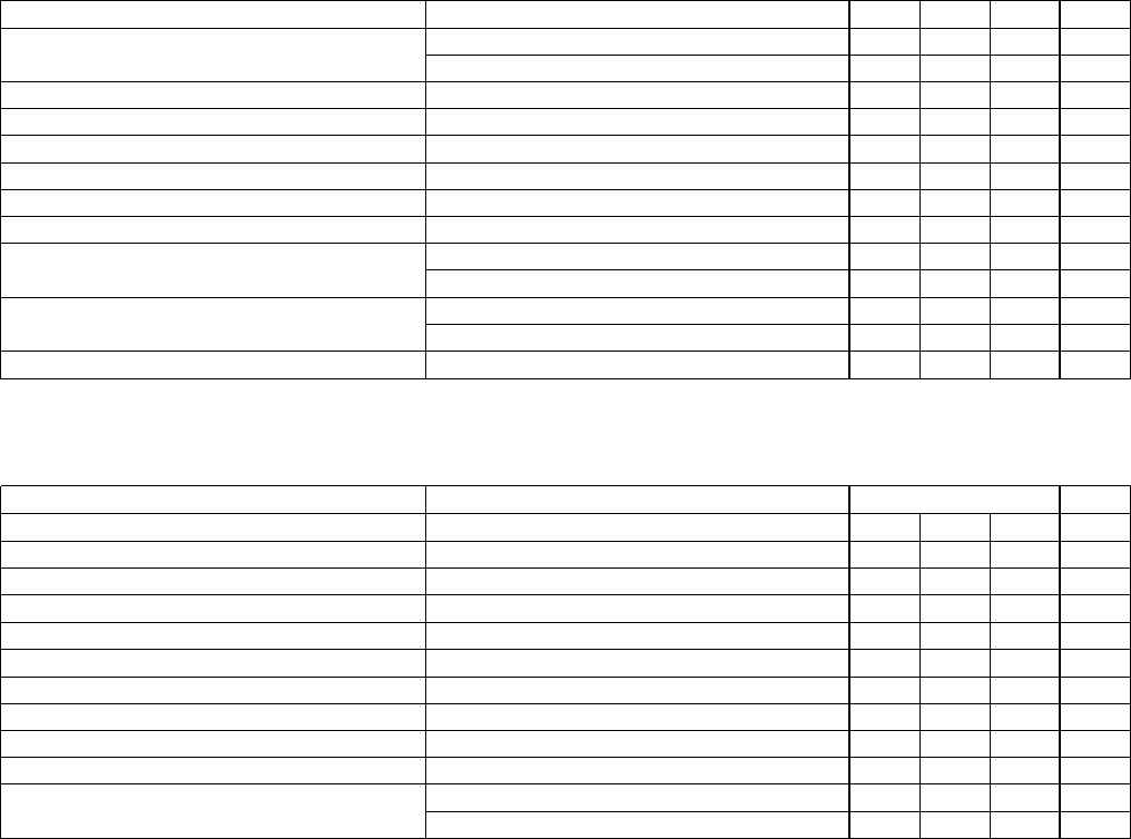
ABSOLUTE MAXIMUM RATINGS
N-Pkg J-Pkg T-Pkg
Supply Voltage, V
IN
. . . . . . . . . . . . . . . . . . . . . . . . . . . . . . . . 40V . . . . . . . . . . . . . . . . . . . 40V . . . . . . . . . . . . . . . . . . . 40V
Collector Supply Voltage, V
C
. . . . . . . . . . . . . . . . . . . . . . . . . 40V . . . . . . . . . . . . . . . . . . . 40V . . . . . . . . . . . . . . . . . . . 40V
Output Current (Source or Sink)
Steady-State. . . . . . . . . . . . . . . . . . . . . . . . . . . . . . . . . . ±500mA. . . . . . . . . . . . . . . . ±500mA. . . . . . . . . . . . . . . . . ±1.0A
Peak Transient . . . . . . . . . . . . . . . . . . . . . . . . . . . . . . . . . ±1.5A. . . . . . . . . . . . . . . . . . ±1.0A. . . . . . . . . . . . . . . . . . ±2.0A
Capacitive Discharge Energy . . . . . . . . . . . . . . . . . . . . . . 20µJ. . . . . . . . . . . . . . . . . . . . 15µJ. . . . . . . . . . . . . . . . . . . . 50µJ
Digital Inputs (See Note) . . . . . . . . . . . . . . . . . . . . . . . . . . . . 5.5V. . . . . . . . . . . . . . . . . . . 5.5V. . . . . . . . . . . . . . . . . . . 5.5V
Power Dissipation at T
A
= 25°C (See Note) . . . . . . . . . . . . . . 1W. . . . . . . . . . . . . . . . . . . . 1W. . . . . . . . . . . . . . . . . . . . 3W
Power Dissipation at T
A
(Leads/Case) = 25°C (See Note) . . . 3W. . . . . . . . . . . . . . . . . . . . 2W . . . . . . . . . . . . . . . . . . . 25W
Operating Temperature Range . . . . . . . . . . . . . . . . . . . . 0°C to +70°C . . . . . . . . . . -55°C to +125°C . . . . . . . . . . 0°C to +70°C
Storage Temperature Range . . . . . . . . . . . . . . . . . . . . -65°C to +150°C . . . . . . . . . -65°C to +150°C . . . . . . . . . -65°C to +150°C
Lead Temperature (Soldering, 10 seconds) . . . . . . . . . . . . . 300°C . . . . . . . . . . . . . . . . . 300°C . . . . . . . . . . . . . . . . . 300°C
Note: All currents are positive into, negative out of the specified terminal.
Digital Drive can exceed 5.5V if input current is limited to 10mA
Consult Packaging Section of Databook for thermal limitations and considerations of package.
UC1705
UC2705
UC3705
TYPICAL SWITCHING CHARACTERISTICS:
PARAMETERS TEST CONDITIONS OUTPUT CL = UNIT
From Inv. Input to Output:
open 1.0 2.2 nF
Rise Time Delay 60 60 60 ns
10% to 90% Rise 20 40 60 ns
Fall Time Delay 60 60 60 ns
90% to 10% Fall 25 40 50 ns
From N. I. Input to Output:
Rise Time Delay 90 90 90 ns
10% to 90% Rise 20 40 60 ns
Fall Time Delay 60 60 60 ns
90% to 10% Fall 25 40 50 ns
V
C Cross-Conduction
Current Spike Duration
Ouput Rise 25 ns
Output Fall 0 ns
PARAMETERS TEST CONDITIONS MIN TYP MAX UNITS
V
S Supply Current VS = 40V, (Outputs High, T Pkg) 6 8 mA
V
S = 40V, (Outputs Low, T Pkg) 8 12 mA
V
C Supply Current (N, J Only) VC = 40V, Outputs Low 2 4 mA
V
C Leakage Current (N, J Only) VS = 0, VC = 30V 0.05 0.1 mA
Digital Input Low Level 0.8 V
Digital Input High Level 2.2 V
Input Current V
I = 0 -0.6 -1.0 mA
Input Leakage V
I = 5V 0.05 0.1 mA
Output High Sat., V
C-VO IO = -50mA 2.0 V
I
O = -500mA 2.5 V
Output Low Sat., V
O IO = 50mA 0.4 V
I
O = 500mA 2.5 V
Thermal Shutdown 155 °C
VS = VC = 20V, TA = 25°C. Delays measured to 10% output change.
Unless otherwise stated, these specifications apply for T
A = -55°C to +125°C for
the UC1705, -25°C to +85°C for the UC2705, and 0°C to +70°C for the UC3705;
VS = VC = 20V, TA =TJ.
ELECTRICAL CHARACTERISTICS: