TLC556, TLC556Y
DUAL LinCMOS TIMERS
SLFS047B – FEBRUARY 1984 – REVISED SEPTEMBER 1997
1
POST OFFICE BOX 655303 • DALLAS, TEXAS 75265
Very Low Power Consumption ...2 mW
Typ at V
DD
= 5 V
Capable of Operation in Astable Mode
CMOS Output Capable of Swinging Rail to
Rail
High Output-Current Capability
Sink 100 mA Typ
Source 10 mA Typ
Output Fully Compatible With CMOS, TTL,
and MOS
Low Supply Current Reduces Spikes
During Output Transitions
Single-Supply Operation From 2 V to 15 V
Functionally interchangeable With the
NE556; Has Same Pinout
description
The TLC556 series are monolithic timing circuits
fabricated using the TI LinCMOS process, which
provides full compatibility with CMOS, TTL, and
MOS logic and operates at frequencies up to
2 MHz. Accurate time delays and oscillations are
possible with smaller, less-expensive timing
capacitors than the NE556 because of the high
input impedance. Power consumption is low
across the full range of power supply voltages.
Like the NE556, the TLC556 has a trigger level
approximately one-third of the supply voltage and
a threshold level approximately two-thirds of the supply voltage. These levels can be altered by use of the control
voltage terminal. When the trigger input falls below the trigger level, the flip-flop is set and the output goes high.
If the trigger input is above the trigger level and the threshold input is above the threshold level, the flip-flop is
reset and the output is low. The reset input can override all other inputs and can be used to initiate a new timing
cycle. If the reset input is low, the flip-flop is reset and the output is low. Whenever the output is low, a
low-impedance path is provided between the discharge terminal and ground.
While the CMOS output is capable of sinking over 100 mA and sourcing over 10 mA, the TLC556 exhibits greatly
reduced supply-current spikes during output transitions. This minimizes the need for the large decoupling
capacitors required by the NE556.
These devices have internal electrostatic-discharge (ESD) protection circuits that prevent catastrophic failures
at voltages up to 2000 V as tested under MIL-STD-883C, Method 3015. However, care should be exercised in
handling these devices, as exposure to ESD may result in degradation of the device parametric performance.
All unused inputs should be tied to an appropriate logic level to prevent false triggering.
The TLC556C is characterized for operation from 0°C to 70°C. The TLC556I is characterized for operation from
–40°C to 85°C. The TLC556M is characterized for operation over the full military temperature range of –55°C
to 125°C.
Copyright 1997, Texas Instruments Incorporated
PRODUCTION DATA information is current as of publication date.
Products conform to specifications per the terms of Texas Instruments
standard warranty. Production processing does not necessarily include
testing of all parameters.
LinCMOS is a trademark of Texas Instruments Incorporated.
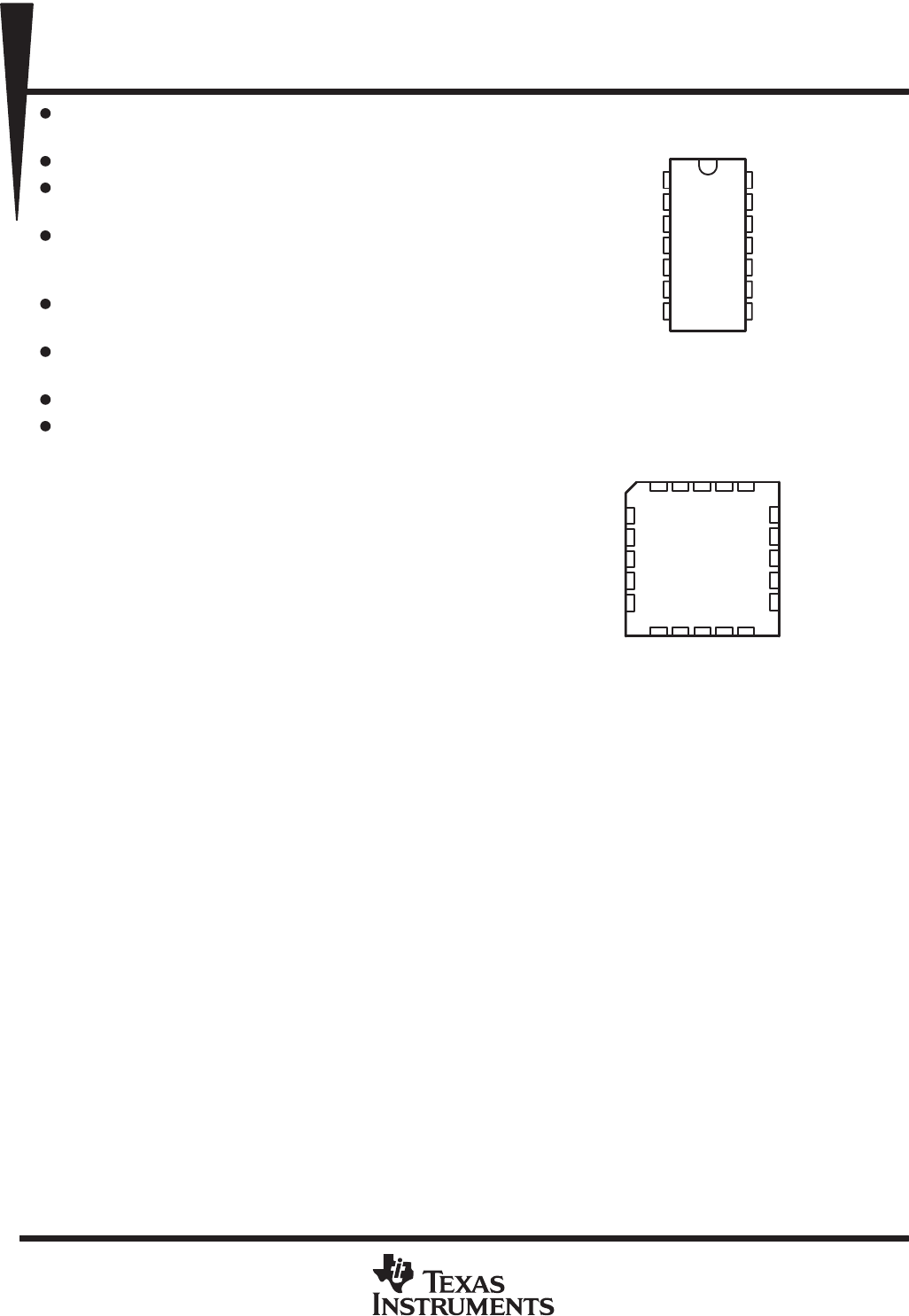
1 DISCH
1 THRES
1 CONT
1 RESET
1 OUT
1 TRIG
GND
1
2
3
4
5
6
7
14
13
12
11
10
9
8
V
DD
2 DISCH
2 THRES
2 CONT
2 RESET
2 OUT
2 TRIG
D, J, OR N PACKAGE
(TOP VIEW)
3 2 1 20 19
910111213
4
5
6
7
8
18
17
16
15
14
2 THRES
NC
2 CONT
NC
2 RESET
1 CONT
NC
1 RESET
NC
1 OUT
FK PACKAGE
(TOP VIEW)
1 THRES
1 DISCH
NC
2 TRIG
2 OUT
V
2 DISCH
1 TRIG
GND
NC
NC–No internal connection
DD


