Closed Dec 25th-26th
800-300-1968
We Stock Hard to Find Parts
My Account
|
My Orders
|
My Cart
Questions?
(800) 300-1968
Register
(current)
My Account
(current)
My Orders
(current)
My Cart
(current)
Categories
(current)
Manufacturers
Request a Quote
Sell Your Excess
Consignment
Quality Assurance
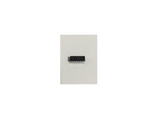
ULN2003AIDR
Part #
ULN2003AIDR
Description
Trans Darlington NPN 50V 0.5A16-Pin SOIC T/R - Tape and R
Category
IC
Availability
Out of Stock
Qty
0
Qty
Price
1 +
$0.13690
Related Items
SGS Thomson
IC
ULN2001A
$0.24771
STMicroelectronics
IC
ULN2002A
$0.09255
Motorola Corp
IC
ULN2003A
$0.22325
Texas Instruments
IC
ULN2003AD
$0.16082
Texas Instruments
IC
ULN2003ADR
$0.27311
Texas Instruments
IC
ULN2003AJ/883B
$2.58786