Closed Dec 25th-26th
800-300-1968
We Stock Hard to Find Parts
My Account
|
My Orders
|
My Cart
Questions?
(800) 300-1968
Register
(current)
My Account
(current)
My Orders
(current)
My Cart
(current)
Categories
(current)
Manufacturers
Request a Quote
Sell Your Excess
Consignment
Quality Assurance
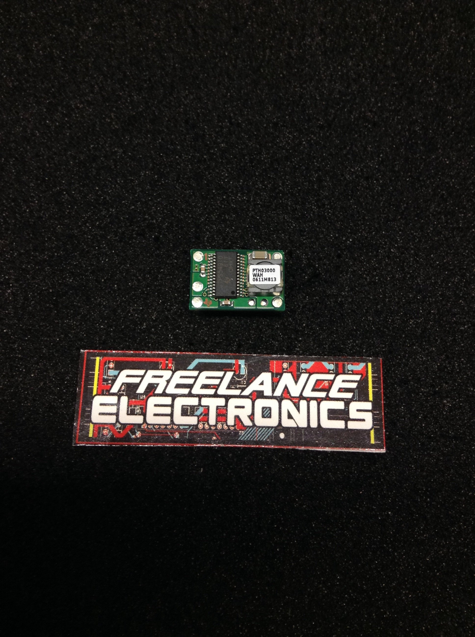
PTH03000WAH
Part #
PTH03000WAH
Description
6A 3.3V INPUT WIDE-OUTPUT PLUG-IN PWR MO
Category
MODULE
Availability
In Stock
Qty
6
Qty
Price
1 - 1
$15.74052
2 - 2
$12.52087
3 - 3
$11.80539
4 - 5
$10.97067
6 +
$9.77820
Manufacturer
Available
Qty
Texas Instruments
Freelance Stock:
4
Ships Immediately
Texas Instruments
Date Code: 0414
Freelance Stock:
2
Ships Immediately
Add to Cart
Related Items
Texas Instruments
MODULE
PTH03010WAH
$24.78615
AMP
MODULE
001405-301-00
SYLVANIA
MODULE
02-900119
Military Spec
MODULE
02-90461-1
DATATRONICS
MODULE
04WJ3SOCN
DELTA ELECTRONICS
MODULE
06A2D
$4.93300