Closed Dec 25th-26th
800-300-1968
We Stock Hard to Find Parts
My Account
|
My Orders
|
My Cart
Questions?
(800) 300-1968
Register
(current)
My Account
(current)
My Orders
(current)
My Cart
(current)
Categories
(current)
Manufacturers
Request a Quote
Sell Your Excess
Consignment
Quality Assurance
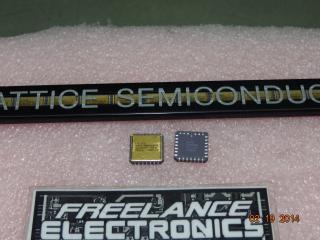
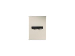
GAL22V10D-15LJ
Part #
GAL22V10D-15LJ
Description
IC CPLD 10MC 15NS 28PLCC
Category
IC
Availability
Out of Stock
Qty
0
Qty
Price
1 +
$6.83920
Related Items
Lattice Semiconductor
IC
GAL22V10-20LR/883C
$45.00205
National Semiconductor Corp
IC
GAL22V10-25LNC
$7.85344
Lattice Semiconductor
IC
GAL22V10-25LP
$5.00000
Lattice Semiconductor
IC
GAL22V100-7LP1
$68.88911
Lattice Semiconductor
IC
GAL22V10B-15LP
$8.03608
Lattice Semiconductor
IC
GAL22V10B-15LR/883