Closed Dec 25th-26th
800-300-1968
We Stock Hard to Find Parts
My Account
|
My Orders
|
My Cart
Questions?
(800) 300-1968
Register
(current)
My Account
(current)
My Orders
(current)
My Cart
(current)
Categories
(current)
Manufacturers
Request a Quote
Sell Your Excess
Consignment
Quality Assurance
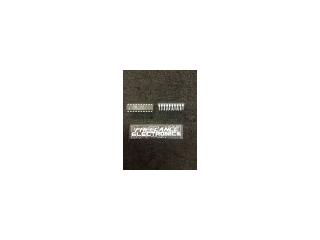
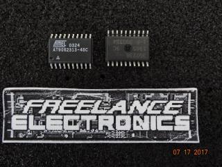
AT90S2313-10PC
Part #
AT90S2313-10PC
Description
10MHZPDIPCOM TEMP5.0V
Category
IC
Availability
Out of Stock
Qty
0
Qty
Price
1 +
$1.92800
Related Items
Atmel
IC
AT90S1200A-4PC
$6.01257
Atmel
IC
AT90S2313-10SC
$4.71206
Atmel
IC
AT90S2313-4PC
$3.69661
Atmel
IC
AT90S2313-4SC
$4.97594
Atmel
IC
AT90S8515-4AC
$12.61420
Fairchild Semiconductor
IC
008-25424
$11.58351