Closed Dec 25th-26th
800-300-1968
We Stock Hard to Find Parts
My Account
|
My Orders
|
My Cart
Questions?
(800) 300-1968
Register
(current)
My Account
(current)
My Orders
(current)
My Cart
(current)
Categories
(current)
Manufacturers
Request a Quote
Sell Your Excess
Consignment
Quality Assurance
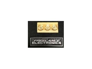
AT-42010
Part #
AT-42010
Description
Trans GP BJT NPN 12V 0.08A 4-Pin Case 100
Category
WAFER DIE
Availability
In Stock
Qty
1
Qty
Price
1 +
$41.88501
Manufacturer
Available
Qty
Hewlett-Packard
Date Code: 9307
Freelance Stock:
1
Ships Immediately
Add to Cart
Related Items
Hewlett-Packard
TRANSISTOR
AT-42085
$11.30200
HEILIND ELECTRONICS
WAFER DIE
09-50-1103
$2.82933
RAYTHEON COMPANY
WAFER DIE
1001796
$16.76391
ATC
WAFER DIE
116ZCB180J100APD
$2.29602
ATC
WAFER DIE
116ZDA510M100APD
$2.34705
Generic
WAFER DIE
1M1109