Freelance Electronics Components Distributor
Closed Dec 25th-26th
800-300-1968
We Stock Hard to Find Parts

STLQ50C50R

Part # STLQ50C50R
Description LDO REG 5V 0.5A 5PIN SOT-323- Tape and Reel
Category VOLTAGE REGULAT
Availability In Stock
Qty 30
Qty Price
1 + $0.09741
Manufacturer Available Qty
SGS Thomson
Date Code: 0946
  • Shipping Freelance Stock: 15
    Ships Immediately
SGS Thomson
  • Shipping Freelance Stock: 15
    Ships Immediately


Technical Document


DISCLAIMER: The information provided herein is solely for informational purposes. Customers must be aware of the suitability of this product for their application, and consider that variable factors such as Manufacturer, Product Category, Date Codes, Pictures and Descriptions may differ from available inventory.

Pin configuration STLQ50XX
4/18
2 Pin configuration
Figure 2. Pin connections (top view)
N/C
OUT
ADJ
GND
STLQ50
IN
N/C
OUT
ADJ
GND
STLQ50
IN
Table 2. Pin description
Pin n° Symbol Note
1
ADJ STLQ50: output voltage adjust
N/C STLQ50xx: not connected
2 GND Ground
3 N/C Not connected
4 IN Input voltage
5 OUT Output voltage
STLQ50XX Maximum ratings
5/18
3 Maximum ratings
Note: Absolute maximum ratings are those values beyond which damage to the device may occur.
Functional operation under these conditions is not implied.
Table 3. Absolute maximum ratings
Symbol Parameter Value Unit
V
I
DC Input voltage -0.3 to +14 V
V
FB
FB voltage -0.3 to +7 V
ESD Human body model (all pins) ±2 kV
T
J
Junction temperature -40 to 150 °C
T
STG
Storage temperature range -55 to 150 °C
Table 4. Thermal data
Symbol Parameter SOT323-5L SOT23-5L Unit
R
thJA
Thermal resistance junction-ambient 331.4
(1)
191
(1)
°C/W
1. This value is referred to a 4-layer PCB, JEDEC standard test board.
Electrical characteristics STLQ50XX
6/18
4 Electrical characteristics
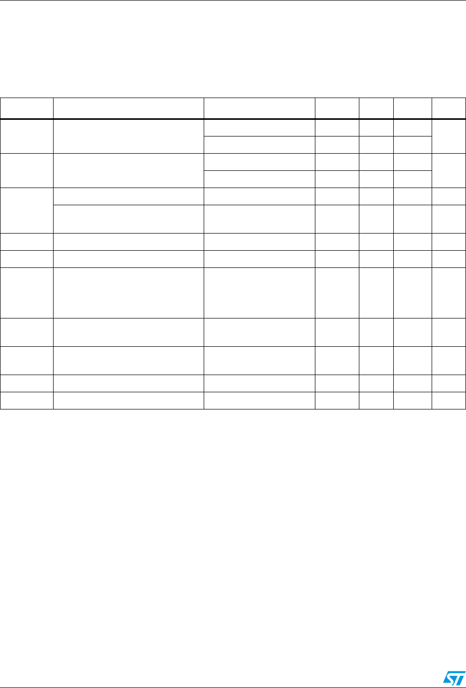
Table 5. Electrical characteristics
(V
I
= V
O(NOM)
+1 V or V
I
= 2.5 V if V
O
+ 1.5 V; T
A
= -40 °C to 125 °C; I
O
= 1 mA; typical values
are at T
A
= 25 °C, C
O
= 1 µF unless otherwise specified)
Symbol Parameter Test conditions Min. Typ. Max. Unit
V
I
Input voltage range
I
O
=20mA 2.3 12
V
I
O
=50mA 2.5 12
I
Q
Quiescent current (Measured on
ground pin, fixed version)
V
I
=5V 3.5 5.0
µA
V
I
=12V 4.1 6.0
V
O
Output voltage range (STLQ50ADJ) 1.222 11 V
Accuracy as percentage of nominal
voltage at T
J
=25°C
-2 +2 %
V
DROP-MAX
Max dropout voltage
(1)
1. V
I
=2.5V when V
O(NOM)
2.1V
I
O
=50mA; 0.4 0.7 V
ΔV
O
Load regulation 1mA < I
O
<50mA 0.15 %/mA
ΔV
O
Line regulation
V
O
=1.5V:
V
O
+1V < V
I
<12V;
V
O
=1.5V:
2.5V < V
I
<12V;
0.3 %/V
SVR Supply voltage rejection
V
RIPPLE
= 0.1V, I
O
= 20mA
f=120Hz
30 dB
eN Output noise voltage
B
W
from 200Hz to
100KHZ; I
O
=10mA
560 µV
RMS
Th Thermal protection 160 °C
I
OMAX
Maximum output current
(2)
2. The maximum power dissipation must not be exceeded, see application information for details.
V
O
=0V 500 mA
PREVIOUS123456NEXT