Closed Dec 25th-26th
800-300-1968
We Stock Hard to Find Parts
My Account
|
My Orders
|
My Cart
Questions?
(800) 300-1968
Register
(current)
My Account
(current)
My Orders
(current)
My Cart
(current)
Categories
(current)
Manufacturers
Request a Quote
Sell Your Excess
Consignment
Quality Assurance
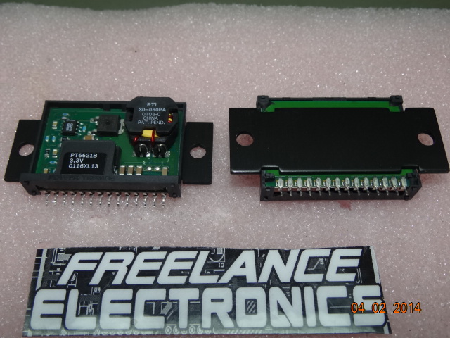
PT6621B
Part #
PT6621B
Description
DC/DC CONVERTER 3.3V 20W
Category
VOLTAGE REGULAT
Availability
In Stock
Qty
336
Qty
Price
1 - 6
$36.33351
7 - 17
$28.90166
18 - 36
$27.25014
37 - 78
$25.32336
79 +
$22.57082
Manufacturer
Available
Qty
Texas Instruments
Date Code: 0000
Freelance Stock:
168
Ships Immediately
Texas Instruments
Date Code: 0116
Freelance Stock:
168
Ships Immediately
Add to Cart
Related Items
Texas Instruments
VOLTAGE REGULAT
PT6625B
$44.58417
Texas Instruments
SWITCH
PT6626B
$36.33351
II
VOLTAGE REGULAT
1122VC
Texas Instruments
VOLTAGE REGULAT
1136VC
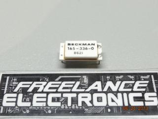
BECKMAN INDUSTRIAL
VOLTAGE REGULAT
165-336-0
$8.00930
Military Spec
VOLTAGE REGULAT
1950114-100