Closed Dec 25th-26th
800-300-1968
We Stock Hard to Find Parts
My Account
|
My Orders
|
My Cart
Questions?
(800) 300-1968
Register
(current)
My Account
(current)
My Orders
(current)
My Cart
(current)
Categories
(current)
Manufacturers
Request a Quote
Sell Your Excess
Consignment
Quality Assurance
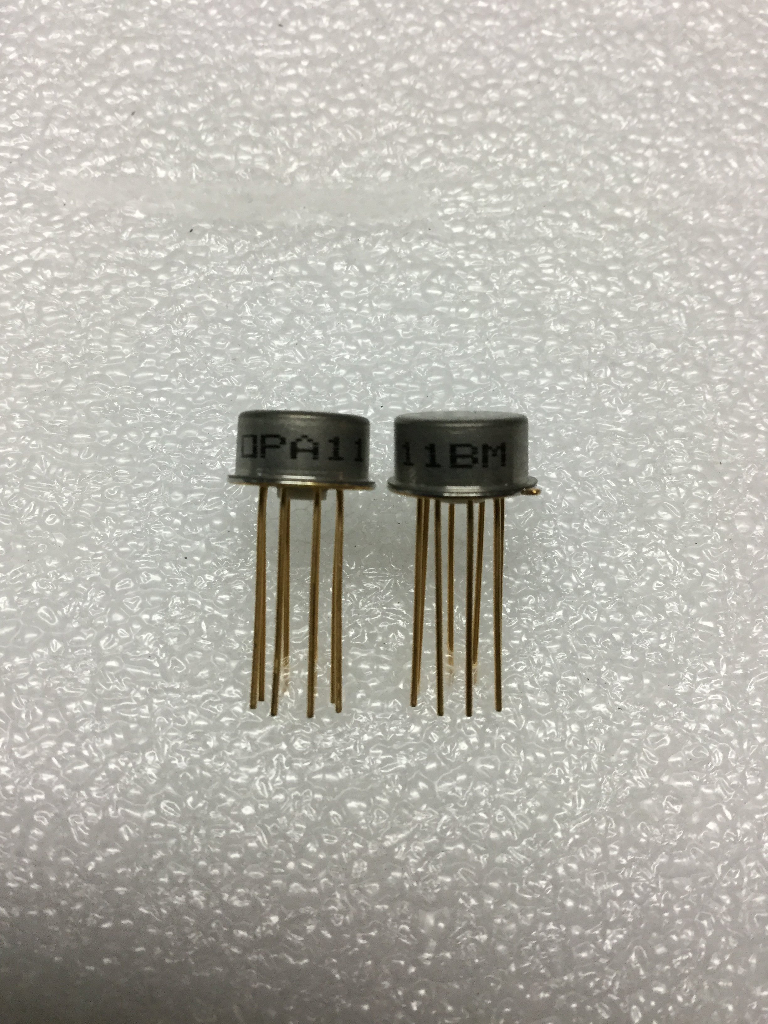
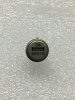
OPA111BM
Part #
OPA111BM
Description
OP AMP, 2MHZ, 500 UV8 PIN
Category
TRANSISTOR
Availability
Out of Stock
Qty
0
Qty
Price
1 +
$35.54276
Related Items
Solitron
TRANSISTOR
001021
$15.91144
Military Spec
TRANSISTOR
0012B
Military Spec
TRANSISTOR
01001
$59.68129
Fairchild Semiconductor
TRANSISTOR
014-505541
Solitron
TRANSISTOR
01714-G641844
SIGNETICS
TRANSISTOR
019-005436
$13.08113