Closed Dec 25th-26th
800-300-1968
We Stock Hard to Find Parts
My Account
|
My Orders
|
My Cart
Questions?
(800) 300-1968
Register
(current)
My Account
(current)
My Orders
(current)
My Cart
(current)
Categories
(current)
Manufacturers
Request a Quote
Sell Your Excess
Consignment
Quality Assurance
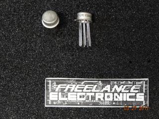
LM193H
Part #
LM193H
Description
Comparator Dual ±18V/36V 8-Pin TO-99 Box - BLK
Category
TRANSISTOR
Availability
Out of Stock
Qty
0
Qty
Price
1 +
$6.94682
Related Items
National Semiconductor Corp
TRANSISTOR
LM193AH/883QS
$24.02788
National Semiconductor Corp
TRANSISTOR
LM193H/883B
$18.09000
National Semiconductor Corp
TRANSISTOR
LM193H/883C
$19.28657
National Semiconductor Corp
TRANSISTOR
LM193H/883QS
$19.28550
National Semiconductor Corp
IC
LM193AH
$6.67959
National Semiconductor Corp
Microcircuit
LM193AH/883C
$12.17587