Closed Dec 25th-26th
800-300-1968
We Stock Hard to Find Parts
My Account
|
My Orders
|
My Cart
Questions?
(800) 300-1968
Register
(current)
My Account
(current)
My Orders
(current)
My Cart
(current)
Categories
(current)
Manufacturers
Request a Quote
Sell Your Excess
Consignment
Quality Assurance
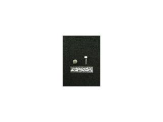
JANTX4N24
Part #
JANTX4N24
Description
OPTOISO 1KV TRANS W/BASE TO78-6
Category
TRANSISTOR
Availability
Out of Stock
Qty
0
Qty
Price
1 +
$9.76528
Related Items
NAE
TRANSISTOR
JANTX1N3011
Infineon
TRANSISTOR
JANTX1N3337B
$627.03963
RAYTHEON SYSTEMS
TRANSISTOR
JANTX1N5109
$55.28821
NES UNITRODE
TRANSISTOR
JANTX1N6492
$47.64420
Generic
TRANSISTOR
JANTX2N04A
Microsemi Corp
TRANSISTOR
JANTX2N1132
$124.39849