Freelance Electronics Components Distributor
Closed Dec 25th-26th
800-300-1968
We Stock Hard to Find Parts

JANTX2N6794

Part # JANTX2N6794
Description 
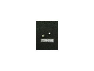
TRANS MOSFET N-CH 500V 1.5A 3PIN TO-39 - Bulk
Category TRANSISTOR
Availability In Stock
Qty 15
Qty Price
1 - 3 $12.37327
4 - 6 $9.84237
7 - 9 $9.27995
10 - 12 $8.62379
13 + $7.68643
Manufacturer Available Qty
Date Code: 8600
  • Shipping Freelance Stock: 15
    Ships Immediately


Technical Document


DISCLAIMER: The information provided herein is solely for informational purposes. Customers must be aware of the suitability of this product for their application, and consider that variable factors such as Manufacturer, Product Category, Date Codes, Pictures and Descriptions may differ from available inventory.

Product Summary
Part Number BVDSS RDS(on) ID
JANTX2N6794
JANTXV2N6794
Features:
Avalanche Energy Rating
Dynamic dv/dt Rating
Simple Drive Requirements
Ease of Paralleling
Hermetically Sealed
N-CHANNEL
Provisional Data Sheet No. PD-9.429B
500 Volt, 3.0
HEXFET
HEXFET technology is the key to International
Rectifier’s advanced line of power MOSFET transis-
tors. The efficient geometry achieves very low on-
state resistance combined with high transconductance.
HEXFET transistors also feature all of the well-es-
tablish advantages of MOSFETs, such as voltage
control, very fast switching, ease of paralleling and
electrical parameter temperature stability. They are
well-suited for applications such as switching power
supplies, motor controls, inverters, choppers, audio
amplifiers, and high energy pulse circuits, and virtu-
ally any application where high reliability is required.
JANTX2N6794
JANTXV2N6794
[REF:MIL-PRF-19500/555]
[GENERIC:IRFF420]
HEXFET
®
POWER MOSFET
Absolute Maximum Ratings
Parameter JANTX2N6794, JANTXV2N6794 Units
I
D
@ V
GS
= 10V, T
C
= 25°C Continuous Drain Current 1.5
I
D
@ V
GS
= 10V, T
C
= 100°C Continuous Drain Current 1.0
I
DM
Pulsed Drain Current 6.0
P
D
@ T
C
= 25°C Max. Power Dissipation 20 W
Linear Derating Factor 0.16 W/K
V
GS
Gate-to-Source Voltage ±20 V
dv/dt Peak Diode Recovery dv/dt 3.5
V/ns
T
J
Operating Junction -55 to 150
T
STG
Storage Temperature Range
Lead Temperature 300
(0.063 in. (1.6mm) from
case for 10.5 seconds)
Weight 0.98 (typical) g
o
C
A
1.5A
3.0500V
Next Data SheetIndex
Previous Datasheet
To Order
Thermal Resistance
Parameter Min. Typ. Max. Units Test Conditions
R
thJC
Junction-to-Case 6.25
R
thJA
Junction-to-Ambient 175 K/W Typical socket mount
Source-Drain Diode Ratings and Characteristics
Parameter Min. Typ. Max. Units Test Conditions
I
S
Continuous Source Current (Body Diode) 1.5 Modified MOSFET symbol showing the
I
SM
Pulse Source Current (Body Diode) 6.0 integral reverse p-n junction rectifier.
V
SD
Diode Forward Voltage 1.2 V T
j
= 25°C, I
S
= 1.5A, V
GS
= 0V
t
rr
Reverse Recovery Time 900 ns T
j
= 25°C, I
F
= 1.5A, di/dt 100A/µs
Q
RR
Reverse Recovery Charge 5.9 µCV
DD
50V
t
on
Forward Turn-On Time
Intrinsic turn-on time is negligible. Turn-on speed is substantially controlled by L
S
+ L
D
.
Electrical Characteristics @ Tj = 25°C (Unless Otherwise Specified)
Parameter Min. Typ. Max. Units Test Conditions
BV
DSS
Drain-to-Source Breakdown Voltage 500 V V
GS
= 0V, I
D
= 1.0 mA
BV
DSS
/T
J
Temperature Coefficient of Breakdown 0.43 V/°C Reference to 25°C, I
D
= 1.0 mA
Voltage
R
DS(on)
Static Drain-to-Source 3.0 V
GS
= 10V, I
D
= 1.0A
On-State Resistance 3.45 V
GS
= 10V, I
D
= 1.5A
V
GS(th)
Gate Threshold Voltage 2.0 4.0 V V
DS
= V
GS
, I
D
= 250µA
g
fs
Forward Transconductance 1.0 S ( )V
DS
> 15V, I
DS
= 1.0A
I
DSS
Zero Gate Voltage Drain Current 25 V
DS
= 0.8 x Max Rating,V
GS
= 0V
250 V
DS
= 0.8 x Max Rating
V
GS
= 0V, T
J
= 125°C
I
GSS
Gate-to-Source Leakage Forward 100 V
GS
= 20V
I
GSS
Gate-to-Source Leakage Reverse -100 V
GS
= -20V
Q
g
Total Gate Charge 7.3 16.7 V
GS
= 10V, I
D
= 1.5A
Q
gs
Gate-to-Source Charge 0.1 3.0 V
DS
= Max. Rating x 0.5
Q
gd
Gate-to-Drain (“Miller”) Charge 3.7 8.7 see figures 6 and 13
t
d(on)
Turn-On Delay Time 40 V
DD
= 250V, I
D
= 1.5A,
t
r
Rise Time 30 R
G
= 7.5, VGS = 10V
t
d(off)
Turn-Off Delay Time 60
t
f
Fall Time 30 see figure 10
L
D
Internal Drain Inductance 5.0
L
S
Internal Source Inductance 15
C
iss
Input Capacitance 350 V
GS
= 0V, V
DS
= 25V
C
oss
Output Capacitance 80 f = 1.0 MHz
C
rss
Reverse Transfer Capacitance 35 see figure 5
JANTX2N6794, JANTXV2N6794 Device
µA
nC
pF
nH
ns
Measured from the
drain lead, 6mm (0.25
in.) from package to
center of die.
Measured from the
source lead, 6mm
(0.25 in.) from package
to source bonding pad.
Modified MOSFET
symbol showing the
internal inductances.
nA
A
Next Data SheetIndex
Previous Datasheet
To Order
Fig. 1 — Typical Output Characteristics
T
C
= 25°C
Fig. 2 — Typical Output Characteristics
T
C
= 150°C
Fig. 3 — Typical Transfer Characteristics
Fig. 4 — Normalized On-Resistance Vs.Temperature
Fig. 5 — Typical Capacitance Vs. Drain-to-Source
Voltage
Fig. 6 — Typical Gate Charge Vs. Gate-to-Source
Voltage
JANTX2N6794, JANTXV2N6794 Device
To Order
Next Data SheetIndex
Previous Datasheet
12NEXT