Closed Dec 25th-26th
800-300-1968
We Stock Hard to Find Parts
My Account
|
My Orders
|
My Cart
Questions?
(800) 300-1968
Register
(current)
My Account
(current)
My Orders
(current)
My Cart
(current)
Categories
(current)
Manufacturers
Request a Quote
Sell Your Excess
Consignment
Quality Assurance
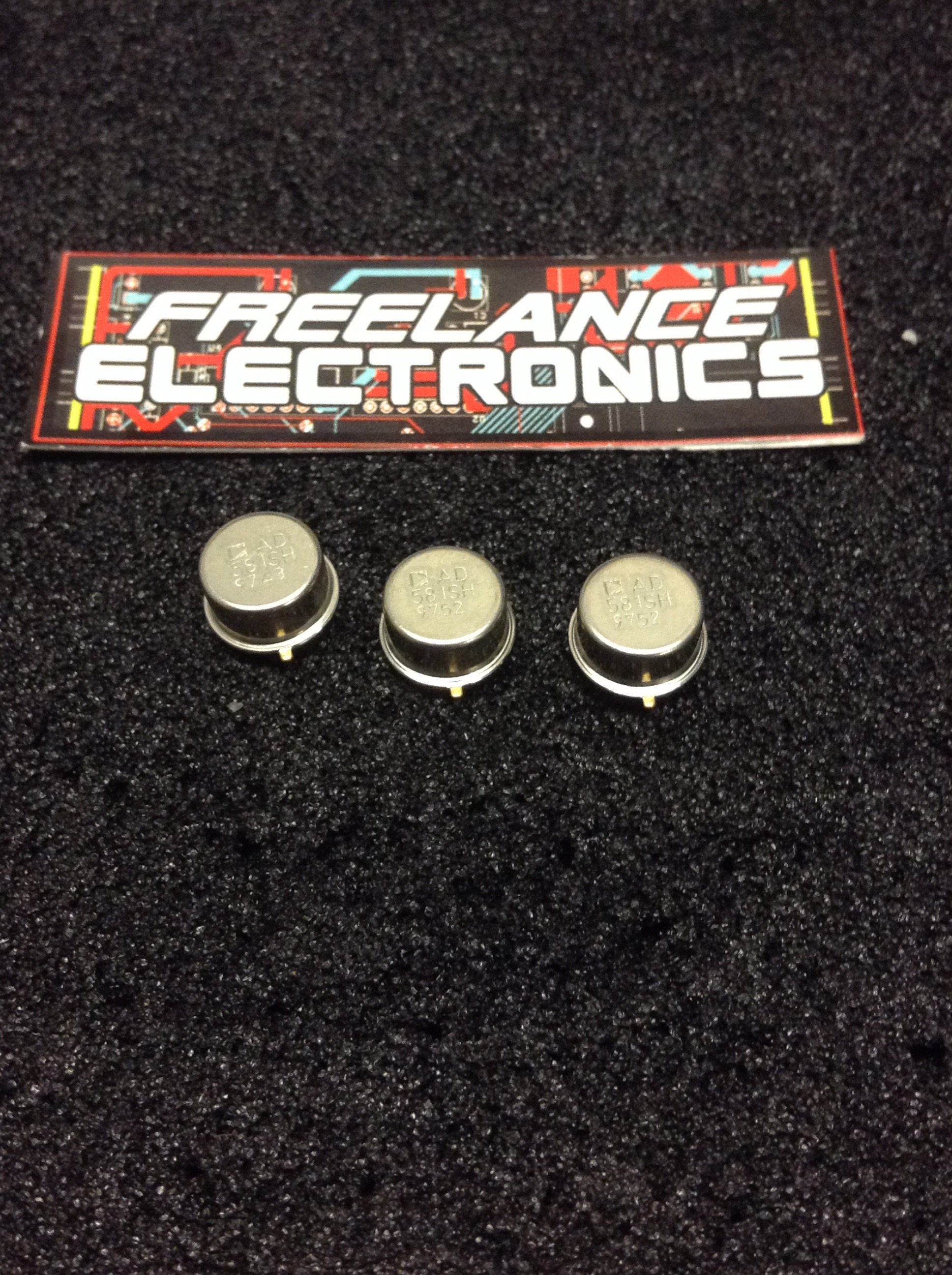
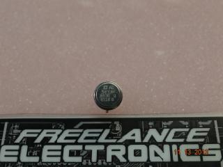
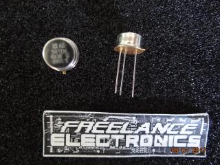
AD581SH
Part #
AD581SH
Description
IC - 10V REFERENCE IC
Category
TRANSISTOR
Availability
Out of Stock
Qty
0
Qty
Price
1 +
$13.18738
Related Items
Linear Technology
TRANSISTOR
AD581SH/883
$70.47396
Analog Devices
TRANSISTOR
AD581TH
$34.77453
Analog Devices
TRANSISTOR
AD581UH/883B
$119.71987
Analog Devices
IC
AD581LH
$20.26077
Analog Devices
IC
AD581TH/883B
$43.59045
MAXIM
Microcircuit
AD581UH
$45.11630