Closed Dec 25th-26th
800-300-1968
We Stock Hard to Find Parts
My Account
|
My Orders
|
My Cart
Questions?
(800) 300-1968
Register
(current)
My Account
(current)
My Orders
(current)
My Cart
(current)
Categories
(current)
Manufacturers
Request a Quote
Sell Your Excess
Consignment
Quality Assurance
A2075
Part #
A2075
Description
Category
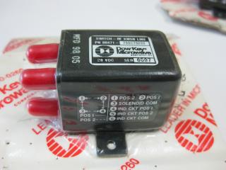
SWITCH
Availability
In Stock
Qty
93
Qty
Price
1 - 7
$19.33770
8 - 19
$15.38226
20 - 37
$14.50327
38 - 57
$13.47779
58 +
$12.01281
Manufacturer
Available
Qty
Military Spec
Freelance Stock:
1
Ships Immediately
Military Spec
Freelance Stock:
1
Ships Immediately
THERMODISC
Date Code: 7908
Freelance Stock:
71
Ships Immediately
THERRM O DISC
Date Code: 7902
Freelance Stock:
20
Ships Immediately
Add to Cart
Related Items
DOW-KEY MICROWAVE CORP
SWITCH
00471
$998.54306
CONCORD ELECTRONICS CORP.
SWITCH
01-1010-1-0210
$6.27480
AMP
SWITCH
01-145510
$18.26381
LICON SWITCH
SWITCH
01-145610
MOLEX
SWITCH
01-55-3004
LICON
SWITCH
01-865210
$54.79145