Freelance Electronics Components Distributor
Closed Dec 25th-26th
800-300-1968
We Stock Hard to Find Parts

7207E

Part # 7207E
Description
Category SWITCH
Availability Out of Stock
Qty 0


Technical Document


DISCLAIMER: The information provided herein is solely for informational purposes. Customers must be aware of the suitability of this product for their application, and consider that variable factors such as Manufacturer, Product Category, Date Codes, Pictures and Descriptions may differ from available inventory.

109
MITSUBISHI MICROCOMPUTERS
M37207MF-XXXSP/FP, M37207M8-XXXSP
M37207EFSP/FP
SINGLE-CHIP 8-BIT CMOS MICROCOMPUTER for VOLTAGE SYNTHESIZER
and ON-SCREEN DISPLAY CONTROLLER
b7 b6 b5 b4 b3 b2 b1 b0
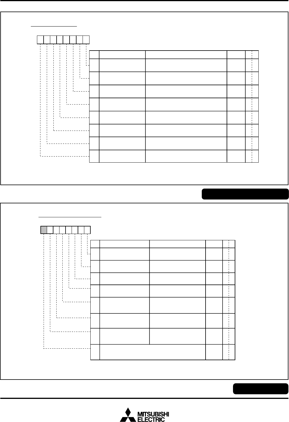
CRT control register 1 (CC) [Address 00EA
16
]
B Name
Functions
After reset
R
W
CRT Control Register 1
0
All-blocks display control
bit (CC0) (See note)
0 : All-blocks display off
1 : All-blocks display on
0
1 Block 1 display control bit
(CC1)
0 : Block 1 display off
1 : Block 1 display on
0
2
0 : Block 2 display off
1 : Block 2 display on
0
Block 2 display control bit
(CC2)
RW
RW
RW
7
0
Note: Display is controlled by logical product (AND) between the all-blocks display
control bit and each block control bit.
Fix this bit to “0.” R W
0
3
0 : Block 3 display off
1 : Block 3 display on
0
Block 3 display control bit
(CC3)
RW
4
0 : Ordinary mode
1 : 1/2-character unit color
specification mode
0
Block 1 color specification
mode switch bit (CC4)
RW
5
0 : Oscillation stopped
1 : Oscillation enabled
0
Display oscillation stop bit
(CC5)
RW
6
0 : Ordinary 256 count
mode
1 : Double count mode
0
Scanning line double count
mode flag(CC6)
RW
CRT Contol Register 1
Color Register n
Address 00EA16
Addresses 00E616, 00E916
b7 b6 b5 b4 b3 b2 b1 b0
Color register n (CO0 to CO3) (n = 0 to 3) [Addresses 00E6
16
to 00E9
16
]
B Name Functions
After reset
R
W
Color Register n
0 0
1 B signal output
selection bit (COn1)
0 : No character is output
1 : Character is output
0
2
G signal output
selection bit (COn2)
0 : No character is output
1 : Character is output
0
3 R signal output
selection bit (COn3)
0 : No character is output
1 : Character is output
0
4
B signal output (background)
selection bit (COn4)
0 : No background color is output
1 : Background color is output
0
5 OUT signal output
control bit (COn5)
0 : Character is output
1 : Blank is output
0
6
G signal output (background)
selection bit (COn6)
0 : No background color is output
1 : Background color is output
0
7
R signal output (background)
selection bit (COn7)
0 : No background color is output
1 : Background color is output
0
(See notes 1,2)
(See notes 1, 2)
Notes 1: When bit 5 = “0” and bit 4 = “1,” there is output same as a character or border output
from the OUT pin.
2: When bit 5 = “0” and bit 4= “0,” there is no output from the OUT pin.
RW
RW
RW
RW
RW
RW
RW
RW
I signal output
selection bit (COn0)
0 : No character is output
1 : Character is output
110
MITSUBISHI MICROCOMPUTERS
M37207MF-XXXSP/FP, M37207M8-XXXSP
M37207EFSP/FP
SINGLE-CHIP 8-BIT CMOS MICROCOMPUTER for VOLTAGE SYNTHESIZER
and ON-SCREEN DISPLAY CONTROLLER
CRT Port Control Register
Display Block Counter
Address 00EB16
Address 00EC16
b7 b6 b5 b4 b3 b2 b1 b0
Display block counter (CBC) [Address 00EB
16
]
B Name Functions
After reset
R
W
Display Block Counter
0
to
3
Number of blocks which are being displayed or has
displayed
(Incremented each time a block is displayed)
Indeterminate
RW
0
Nothing is assigned. These bits are write disable bits.
When these bits are read out, the values are “0.”
R—4
to
7
b7 b6 b5 b4 b3 b2 b1 b0
CRT port control register (CRTP) [Address 00EC
16
]
B Name Functions
After reset
R
W
CRT Port Control Register
0H
SYNC
input polarity
switch bit (HSYC)
0 : Positive polarity
1 : Negative polarity
0
1
0 : Positive polarity
1 : Negative polarity
0
2 R, G, B output polarity
switch bit (R/G/B)
0 : Positive polarity
1 : Negative polarity
0
3 I output polarity switch bit
(I)
0 : Positive polarity
1 : Negative polarity
0
4 OUT output polarity
switch bit (OUT)
0 : Positive polarity
1 : Negative polarity
0
5 R signal output switch bit
(R)
0 : R signal output
1 : MUTE signal output
0
6 G signal output switch bit
(G)
0 : G signal output
1 : MUTE signal output
0
7 B signal output switch bit
(B)
0 : B signal output
1 : MUTE signal output
0
V
SYNC
input polarity
switch bit (VSYC)
RW
RW
RW
RW
RW
RW
RW
RW
111
MITSUBISHI MICROCOMPUTERS
M37207MF-XXXSP/FP, M37207M8-XXXSP
M37207EFSP/FP
SINGLE-CHIP 8-BIT CMOS MICROCOMPUTER for VOLTAGE SYNTHESIZER
and ON-SCREEN DISPLAY CONTROLLER
A-D Control Register 1
Wipe Mode Register
Address 00ED16
Address 00EF16
b7 b6 b5 b4 b3 b2 b1 b0
Wipe mode register (SL) [Address 00ED
16
]
B Name Functions
After reset
R
W
Wipe Mode Register
0, 1 Wipe mode selection bits
(SL0, SL1)
b1 b0
0 0 : Wipe is not available
0 1 : Mode 1
1 0 : Mode 2
1 1 : Mode 3
0
2
Direction mode selection
bits (SL2)
0
RW
RW
7
0
Nothing is assigned. This bit is a write disable bit.
When this bit is read out, the value is indeterminate.
R—
3, 4
Wipe unit selection bits
(SL3, SL4)
0
RW
0: DOWN mode
1: UP mode
b4 b3
0 0 : 1H unit
0 1 : 2H unit
1 0 : 3H unit
1 1 : Do not set
5, 6
Stop mode selection bits
(SL5, SL6)
0
RW
b6 b5
0 0 : Stop at the 312nd H
0 1 : Stop at the 156th H
1 0 : Stop at the 256th H
1 1 : Stop at the 128th H
b7 b6 b5 b4 b3 b2 b1 b0
A-D control register 1 (ADM) [Address 00EF
16
]
B
After reset
RW
A-D Control Register 1
0
to
2
Analog input pin selection
bits
(ADM0 to ADM2)
Name Functions
b2 b1 b0
0 0 0 : AD1
0 0 1 : AD2
0 1 0 : AD3
0 1 1 : AD4
1 0 0 : AD5
1 0 1 : AD6
1 1 0 : AD7
1 1 1 : AD8
4
Storage bit of comparison
result (ADM4)
0:
Input voltage < reference voltage
1:
Input voltage > reference voltage
0
Indeterminate
0
3,
5
to
7
Nothing is assigned. These bits are write disable bits.
When these bits are read out, the values are “0.”
RW
R—
R—
PREVIOUS303132333435363738394041NEXT