Freelance Electronics Components Distributor
Closed Dec 25th-26th
800-300-1968
We Stock Hard to Find Parts

7207E

Part # 7207E
Description
Category SWITCH
Availability Out of Stock
Qty 0


Technical Document


DISCLAIMER: The information provided herein is solely for informational purposes. Customers must be aware of the suitability of this product for their application, and consider that variable factors such as Manufacturer, Product Category, Date Codes, Pictures and Descriptions may differ from available inventory.

106
MITSUBISHI MICROCOMPUTERS
M37207MF-XXXSP/FP, M37207M8-XXXSP
M37207EFSP/FP
SINGLE-CHIP 8-BIT CMOS MICROCOMPUTER for VOLTAGE SYNTHESIZER
and ON-SCREEN DISPLAY CONTROLLER
Serial I/O Mode Register
I
2
C Clock Control Register
Address 00DD16
Address 00DE16
b7 b6 b5 b4 b3 b2 b1 b0
I
2
C clock control register (S2 : address 00DD16)
I
2
C Clock Control Register
0
to
4
SCL frequency control bits
(CCR0 to CCR4)
7
5
6
SCL mode
specification bit
(FAST MODE)
0 : Standard clock mode
1 : High-speed clock mode
0
Standard clock
mode
B Name Functions
After reset
RW
0
0
0
ACK bit
(ACK BIT)
ACK clock bit
(ACK)
0 : ACK is returned.
1 : ACK is not returned.
0 : No ACK clock
1 : ACK clock
High speed
clock mode
Setup disabled Setup disabled
00 to 02
Setup disabled
33303
Setup disabled
25004
100
400 (See note)
05
83.3 16606
500/CCR value 1000/CCR value
...
17.2 34.5
1D
16.6 33.3
1E
16.1
32.3
1F
(at
φ
= 4 MHz, unit : kHz)
Note: At 400 kHz in the high-speed clock mode, the duty is as below .
“0” period : “1” period = 3 : 2
In the other cases, the duty is as below.
“0” period : “1” period = 1 : 1
Setup value of
CCR4–CCR0
RW
RW
RW
RW
b7b6 b5b4b3 b2b1b0
Serial I/O mode register (SM) [Address 00DE
16
]
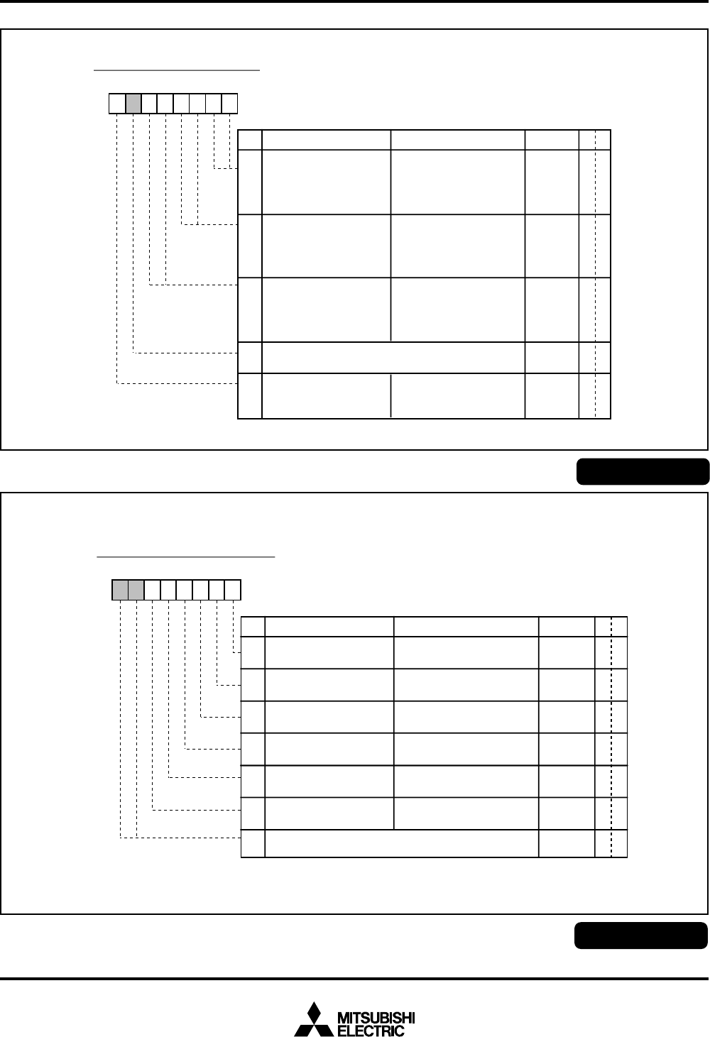
B Name Functions
After reset
RW
Serial I/O Mode Register
0, 1
Internal synchronous
clock selection bits
(SM0, SM1)
(See note 1)
b1 b0
0 0: f(X
IN
)/4 or f(X
CIN
)/4
0 1: f(X
IN
)/16 or f(X
CIN
)/16
1 0: f(X
IN
)/32 or f(X
CIN
)/32
1 1: f(X
IN
)/64 or f(X
CIN
)/64
2
Synchronous clock
selection bit (SM2)
3, 7
Ports P4
0
, P4
1
function selection
bits (SM3, SM7)
P4
0
/S
OUT2
/
SDA3/X
CIN
P4
0
S
OUT2
SDA3
0: External clock
1: Internal clock
0
0
0
RW
RW
RW
4, 6
Ports P4
2
, P4
3
function selection bits
(SM4, SM6)
5
Transfer direction
selection bit (SM5)
0: LSB first
1: MSB first
0RW
P4
1
/S
CLK2
/
SCL3/X
COUT
P4
1
S
CLK2
SCL3
b7
0
1
b3
0
1
P4
2
/S
IN2
/
SDA2/AD8
P4
2
SDA2
P4
2
SDA2
0RW
P4
3
/S
RDY2
/
SCL2/AD7
P4
3
S
RDY2
SDA2
b6
0
1
0
1
b4
0
1
Notes 1: Either f(X
IN
) or f(X
CIN
) is selected by bit 7 of the CPU
mode register.
2: When using ports P4
0
–P4
3
as serial I/O pins, set bit 1 of
the serial control register to “1.”
(See note 2)
(See note 2)
107
MITSUBISHI MICROCOMPUTERS
M37207MF-XXXSP/FP, M37207M8-XXXSP
M37207EFSP/FP
SINGLE-CHIP 8-BIT CMOS MICROCOMPUTER for VOLTAGE SYNTHESIZER
and ON-SCREEN DISPLAY CONTROLLER
Vertical Position Register i
Horizontal Position Register
Addresses 00E116, 00E316
Address 00E016
b7 b6 b5 b4 b3 b2 b1 b0
Horizontal position register (HR) [Address 00E0
16]
B Name Functions
After reset
RW
Horizontal Position Register
0
to
5
6
Horizontal display start
positions (HR0 to HR5)
64 steps (0016 to 3F16)
0
0Nothing is assigned. This bit is a write disable bit.
When this bit is read out, the value is “0.”
RW
R—
0
7
0Fix this bit to “0.” R W
b7 b6 b5 b4 b3 b2 b1 b0
Vertical position register i (CVi) (i = 1 to 3) [Addresses 00E1
16
to 00E3
16
]
B Name Functions
After reset
R
W
Vertical Position Register i
0
to
6
7
Vertical display start positions
128 steps (00
16
to 7F
16
)
Indeterminate
0
(CVi : CVi0 to CVi6)
Nothing is assigned. This bit is a write disable bit.
When this bit is read out, the value is “0.”
RW
R—
108
MITSUBISHI MICROCOMPUTERS
M37207MF-XXXSP/FP, M37207M8-XXXSP
M37207EFSP/FP
SINGLE-CHIP 8-BIT CMOS MICROCOMPUTER for VOLTAGE SYNTHESIZER
and ON-SCREEN DISPLAY CONTROLLER
Border Selection Register
Character Size Register
Address 00E416
Address 00E516
b7 b6 b5 b4 b3 b2 b1 b0
Character size register (CS) [Address 00E4
16
]
B Name Functions
After reset
R
W
Character Size Register
0, 1 Character size of block 1
selection bits
(CS10, CS11)
b1 b0
0 0 : Minimum size
0 1 : Medium size
1 0 : Large size
1 1 : Extra large size
Indeterminate
2, 3
Character size of block 2
selection bits
(CS20, CS21)
Indeterminate
RW
RW
6
Indeterminate
Nothing is assigned. This bit is a write disable bit.
When this bit is read out, the value is indeterminate.
R—
4, 5 Character size of block 2
selection bits
(CS30, CS31)
Indeterminate
RW
7
OUT signal output switch
bit
(CS7)
0 : OUT signal output
1 : MUTE signal output
(See note)
Indeterminate
RW
Note: This erases a video signal on an entire screen.
b3 b2
0 0 : Minimum size
0 1 : Medium size
1 0 : Large size
1 1 : Extra large size
b5 b4
0 0 : Minimum size
0 1 : Medium size
1 0 : Large size
1 1 : Extra large size
b7 b6 b5 b4 b3 b2 b1 b0
Border selection register (MD) [Address 00E5
16
]
B Name Functions
After reset
R
W
Border Selection Register
0 Block 1 OUT output
border selection bit (MD10)
0 : Same output as character output
1 : Border output
Indeterminate
1
Indeterminate
2 Block 2 OUT output
border selection bit (MD20)
0 : Same output as character output
1 : Border output
Indeterminate
RW
RW
RW
0
6, 7
Nothing is assigned. These bits are write disable bits.
When these bits are read out, the values are “0.”
R—
Block 1 OUT output
switch bit (MD11)
0 : Border including character
1 : Border only
3
Indeterminate
RWBlock 2 OUT output
switch bit (MD21)
0 : Border including character
1 : Border only
4 Block 3 OUT output
border selection bit (MD30)
0 : Same output as character output
1 : Border output
Indeterminate
RW
5
Indeterminate
RWBlock 3 OUT output
switch bit (MD31)
0 : Border including character
1 : Border only
PREVIOUS29303132333435363738394041NEXT