Freelance Electronics Components Distributor
Closed Dec 25th-26th
800-300-1968
We Stock Hard to Find Parts

7207E

Part # 7207E
Description
Category SWITCH
Availability Out of Stock
Qty 0


Technical Document


DISCLAIMER: The information provided herein is solely for informational purposes. Customers must be aware of the suitability of this product for their application, and consider that variable factors such as Manufacturer, Product Category, Date Codes, Pictures and Descriptions may differ from available inventory.

103
MITSUBISHI MICROCOMPUTERS
M37207MF-XXXSP/FP, M37207M8-XXXSP
M37207EFSP/FP
SINGLE-CHIP 8-BIT CMOS MICROCOMPUTER for VOLTAGE SYNTHESIZER
and ON-SCREEN DISPLAY CONTROLLER
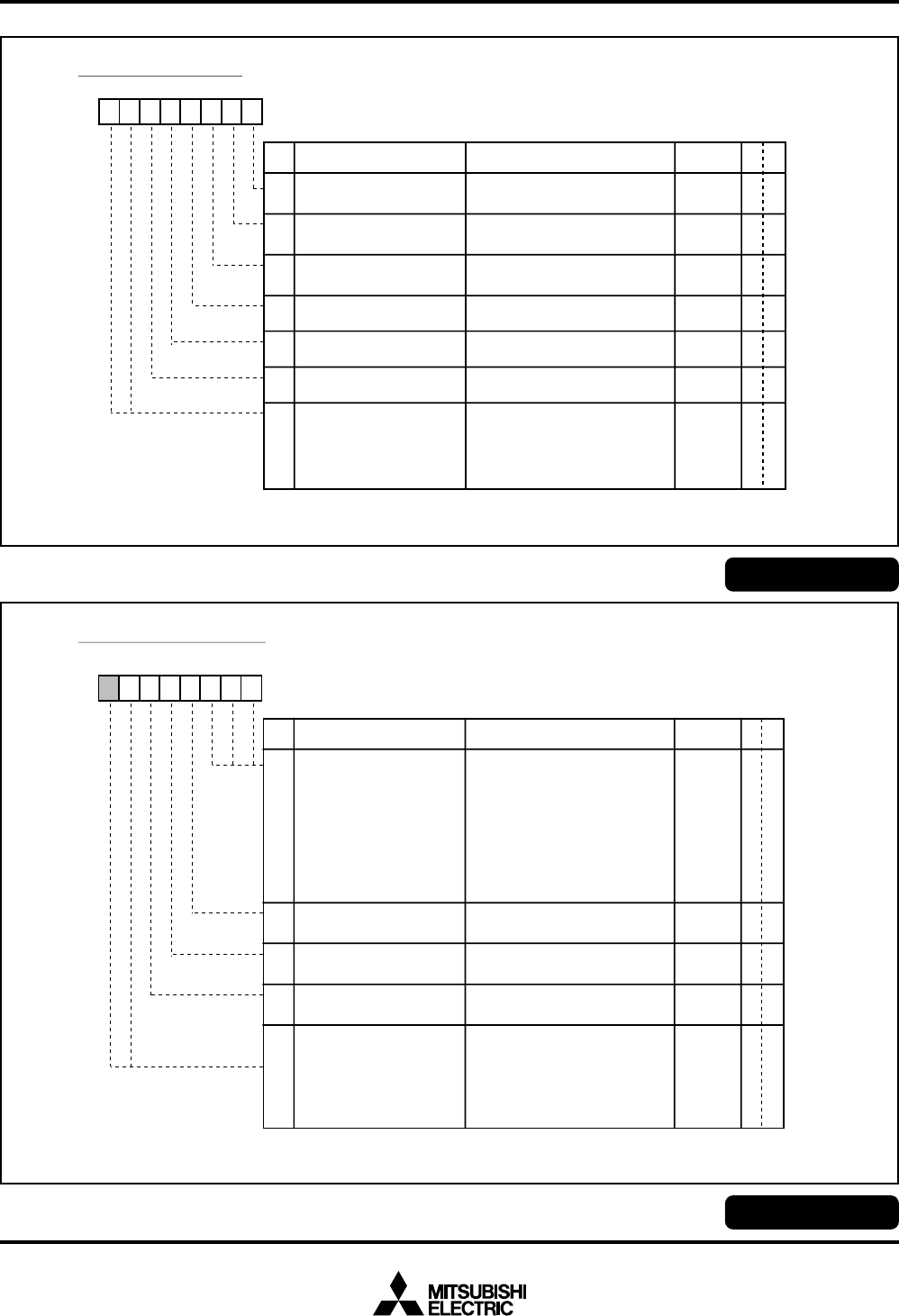
Interrupt Interval Determination Control Register
Address 00D616
Address 00D816
PWM Output Control Register
b7b6 b5b4b3 b2b1b0
PWM output control register 2 (PN) [Address 00D6
B
After reset
RW
PWM Output Control Register 2
Name Functions
16
]
2
3
4
DA output polarity
selection bit (PN3)
0 : Positive polarity
1 : Negative polarity
PWM output polarity
selection bit (PN4)
DA general-purpose
output bit (PN5)
0 : Output LOW
1 : Output HIGH
5
to
7
0
0
0
0
Nothing is assigned. These bits are write disable bits.
When these bits are read out, the values are “0.”
0 : Positive polarity
1 : Negative polarity
RW
RW
RW
R—
0
P6
6
/PWM6 output
selection bit (PN0)
0 : P6
6
output
1 : PWM6 output
0RW
1
P6
7
/PWM7 output
selection bit (PN1)
0 : P6
7
output
1 : PWM7 output
0RW
b7 b6 b5 b4 b3 b2 b1 b0
interrupt interval determination control register (RE) [Address 00D8
16
]
B Name Functions
After reset
R
W
Interrupt Interval Determination Control Register
0 Interrupt interval
determination circuit
operation control bit (RE0)
0 : Stopped
1 : Operating
0
1 Reference clock selection
bit (RE1)
0 : 16 µs
1 : 32 µs
(at f(X
IN
) = 8 MHz)
0
2 External interrupt input
pin selection bit (RE2)
0 : INT1 input
1 : INT2 input
0
3 INT1 pin input polarity
switch bit (RE3)
0 : Positive polarity input
1 : Negative polarity input
0
4 INT2 pin input polarity
switch bit (RE4)
0 : Positive polarity input
1 : Negative polarity input
0
5
to
7
0
RW
RW
RW
RW
RW
R—
Nothing is assigned. These bits are write disable bits.
When these bits are read out, the values are “0.”
104
MITSUBISHI MICROCOMPUTERS
M37207MF-XXXSP/FP, M37207M8-XXXSP
M37207EFSP/FP
SINGLE-CHIP 8-BIT CMOS MICROCOMPUTER for VOLTAGE SYNTHESIZER
and ON-SCREEN DISPLAY CONTROLLER
I
2
C Adress Register
I
2
C Data Shift Register
Address 00D916
Address 00DA16
b7 b6 b5 b4 b3 b2 b1 b0
I C data shift register1(S0) [Address 00D9
16
]
B Functions After reset R W
I C Data Shift Register
0
to
7
This is an 8-bit shift register to store
receive data and write transmit data.
Indeterminate
2
2
Note:
2
To write data into the I C data shift register after setting the MST bit to
“0” (slave mode), keep an interval of 8 machine cycles or more.
Name
D0 to D7
RW
b7 b6 b5 b4 b3 b2 b1 b0
0
Read/write bit
(RBW)
1
to
7
Slave address
(SAD0 to SAD6)
0: Read
1: Write
0
0The address data transmitted from
the master is compared with the
contents of these bits.
I
2
C Address Register
I
2
C address register (S0D) [Address 00DA
16
]
B Name Functions
After reset
RW
R—
RW
105
MITSUBISHI MICROCOMPUTERS
M37207MF-XXXSP/FP, M37207M8-XXXSP
M37207EFSP/FP
SINGLE-CHIP 8-BIT CMOS MICROCOMPUTER for VOLTAGE SYNTHESIZER
and ON-SCREEN DISPLAY CONTROLLER
I
2
C Control Register
I
2
C Status Register
Address 00DC16
Address 00DB16
b7 b6 b5 b4 b3 b2 b1 b0
I
2
C status register (S1) [Address 00DB
16
]
I
2
C Status Register
0
3
4
5
6, 7 b7 b6
0 0 : Slave recieve mode
0 1 : Slave transmit mode
1 0 : Master recieve mode
1 1 : Master transmit mode
1
2
0
0
0
0
0
B Name Functions
After reset
RW
Communication mode
specification bits
(TRX, MST)
0 : Bus free
1 : Bus busy
Bus busy flag (BB)
0 : Interrupt request issued
1 : No interrupt request issued
I
2
C-BUS interface interrupt
request bit (PIN)
0 : Not detected
1 : Detected
Arbitration lost detecting flag
(AL) (See note)
0 : Address mismatch
1 : Address match
Slave address comparison
flag (AAS) (See note)
0 : No general call detected
1 : General call detected
General call detecting flag
(AD0) (See note)
0 : Last bit = “0 ”
1 : Last bit = “1 ”
Last receive bit (LRB)
(See note)
Note : These bits and flags can be read out, but cannnot be written.
Indeterminate
R—
R—
R—
R—
R—
RW
0
RW
b7 b6 b5 b4 b3 b2 b1 b0
0
to
2
Bit counter
(Number of transmit/recieve
bits)
(BC0 to BC2)
b2 b1 b0
0 0 0 : 8
0 0 1 : 7
0 1 0 : 6
0 1 1 : 5
1 0 0 : 4
1 0 1 : 3
1 1 0 : 2
1 1 1 : 1
3
I
2
C-BUS interface use
enable bit (ESO)
0 : Disabled
1 : Enabled
4 Data format selection bit
(ALS)
0 : Addressing mode
1 : Free data format
5
Addressing format selection
bit (10BIT SAD)
0 : 7-bit addressing format
1 : 10-bit addressing format
6, 7 Connection control bits
between I C-BUS interface
and ports
b7 b6 Connection port (See note)
0 0 : None
0 1 : SCL1, SDA1
1 0 : SCL2, SDA2
1 1 : SCL1, SDA1
SCL2, SDA2
0
0
0
0
0
I
2
C control register (S1D : address 00DC16)
I
2
C Control Register
B Name Functions
After reset
RW
Note: When using ports P11-P14 as I C-BUS interface, the output structure changes
automatically from CMOS output to N-channel open-drain output.
2
2
RW
RW
RW
RW
RW
PREVIOUS2829303132333435363738394041NEXT