Freelance Electronics Components Distributor
Closed Dec 25th-26th
800-300-1968
We Stock Hard to Find Parts

7207E

Part # 7207E
Description
Category SWITCH
Availability Out of Stock
Qty 0


Technical Document


DISCLAIMER: The information provided herein is solely for informational purposes. Customers must be aware of the suitability of this product for their application, and consider that variable factors such as Manufacturer, Product Category, Date Codes, Pictures and Descriptions may differ from available inventory.

100
MITSUBISHI MICROCOMPUTERS
M37207MF-XXXSP/FP, M37207M8-XXXSP
M37207EFSP/FP
SINGLE-CHIP 8-BIT CMOS MICROCOMPUTER for VOLTAGE SYNTHESIZER
and ON-SCREEN DISPLAY CONTROLLER
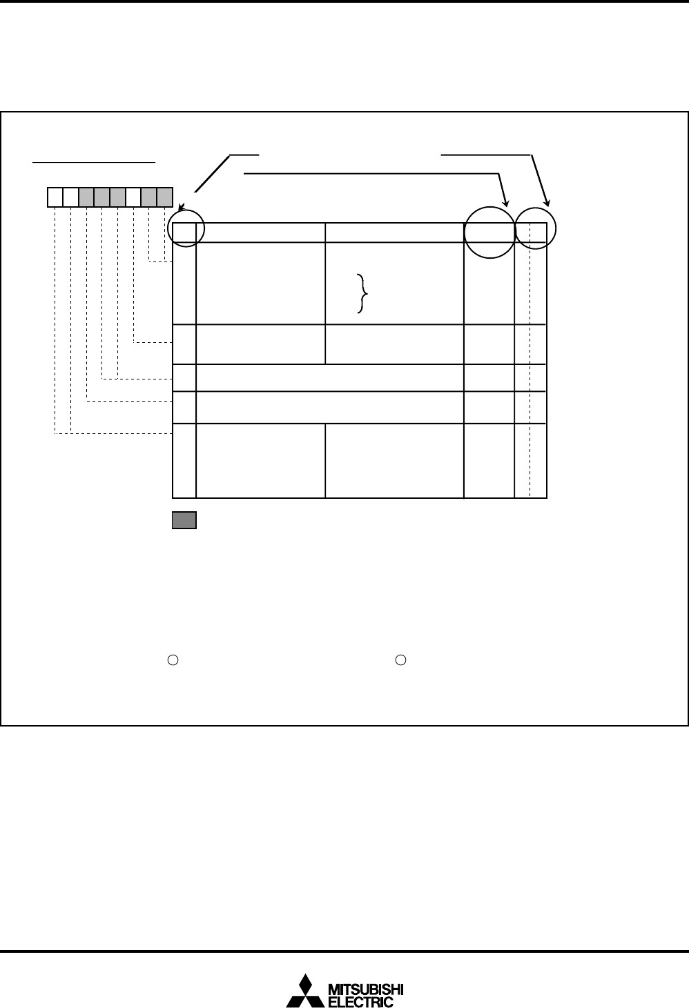
Structure of Register
The figure of each register structure describes its functions, contents
at reset, and attributes as follows:
Values immediately after reset release
Bit attributes
(Note 1)
(Note 2)
Bits
2: Bit attributes••••••The attributes of control register bits are classified into 3 types : read-only, write-only
and read and write. In the figure, these attributes are represented as follows :
: Bit in which nothing is assigned
Notes 1: Values immediately after reset release
0••••••“0” after reset release
1••••••“1” after reset release
?••••••Indeterminate after reset release
••••••Read enabled
••••••Read disabled
R••••••Read
••••••Write enabled
••••••Write disabled
••••••“0” can be set by software, but “1”
cannot be set.
W••••••Write
b7b6 b5b4b3 b2b1b0
B
After reset
RW
CPU Mode Register
0, 1
2
3, 4
0
1
1
Name Functions
Processor mode bits
(CM0, CM1)
0 0: Single-chip mode
0 1:
1 0: Not available
1 1:
Fix these bits to “1.”
0
Stack page selection
bit (Note) (CM2)
1
b1 b0
0: 0 page
1: 1 page
100
5 Nothing is assigned. This bit is write disable bit.
When this bit is read out, the value is “0.”
6, 7 0
Clock switch bits
(CM6, CM7)
0 0: f(X
IN
) = 8 MHz
0 1: f(X
IN
) = 12 MHz
1 0: f(X
IN
) = 16 MHz
1 1: Do not set
b7 b6
CPU mode register (CPUM) (CM) [Address FB
16]
RW
RW
RW
RW
RW
[Example]
101
MITSUBISHI MICROCOMPUTERS
M37207MF-XXXSP/FP, M37207M8-XXXSP
M37207EFSP/FP
SINGLE-CHIP 8-BIT CMOS MICROCOMPUTER for VOLTAGE SYNTHESIZER
and ON-SCREEN DISPLAY CONTROLLER
Port Pi Direction Register
Port P3 Direction Register
Addresses 00C116, 00C316, 00C516, 00CD16
Address 00C716
b7 b6 b5 b4 b3 b2 b1 b0
Port Pi direction register (Di) (i=0,1,2, 6) [Addresses 00C1
16,
00C3
16
, 00C5
16
, 00CD
16
]
B Name Functions
After reset
R
W
Port Pi Direction Register
0 0 : Port Pi
0
input mode
1 : Port Pi
0
output mode
0
1
0 : Port Pi
1
input mode
1 : Port Pi
1
output mode
0
2
0 : Port Pi
2
input mode
1 : Port Pi
2
output mode
0
3 0 : Port Pi
3
input mode
1 : Port Pi
3
output mode
0
4 0 : Port Pi
4
input mode
1 : Port Pi
4
output mode
0
5 0 : Port Pi
5
input mode
1 : Port Pi
5
output mode
0
6 0 : Port Pi
6
input mode
1 : Port Pi
6
output mode
0
7
0 : Port Pi
7
input mode
1 : Port Pi
7
output mode
0
Port Pi direction register
RW
RW
RW
RW
RW
RW
RW
RW
b7 b6 b5 b4 b3 b2 b1 b0
Port P3 direction register (D3) [Address 00C7
16
]
B Name Functions
After reset
RW
Port P3 Direction Register
0 0 : Port P3
0
input mode
1 : Port P3
0
output mode
0
1
0 : Port P3
1
input mode
1 : Port P3
1
output mode
0
2 0 : Port P3
2
input mode
1 : Port P3
2
output mode
0
0
Port P3 direction register
Nothing is assigned. This bit is a write disable bit.
When this bit is read out, the value is “0.”
RW
RW
RW
R—
3
0 : Port P3
3
input mode
1 : Port P3
3
output mode
0RW
6
0RW
7
0 : Port P3
4
input mode
1 : Port P3
4
output mode
0RW
0 : Port P3
5
input mode
1 : Port P3
5
output mode
0RW
4
5
0 : Port P3
6
input mode
1 : Port P3
6
output mode
102
MITSUBISHI MICROCOMPUTERS
M37207MF-XXXSP/FP, M37207M8-XXXSP
M37207EFSP/FP
SINGLE-CHIP 8-BIT CMOS MICROCOMPUTER for VOLTAGE SYNTHESIZER
and ON-SCREEN DISPLAY CONTROLLER
Port P5 Control Register
PWM Output Control Register 1
Address 00CB16
Address 00D516
b7 b6 b5 b4 b3 b2 b1 b0
Port P5 control register (D5) [Address 00CB
16
]
B Name Functions
After reset
R
W
Port P5 Control Register
0
0
2
3 0 : G signal output
1 : Port P5
3
output
0
0
R—
RW
RW
RW
0, 1,
7
Port P5
3
output signal
selection bit (G)
4
0 : B signal output
1 : Port P5
4
output
0RWPort P5
4
output signal
selection bit (B)
0RW
0 : R signal output
1 : Port P5
2
output
Port P5
2
output signal
selection bit (R)
5 0 :
I/TIM1 OVERFLOW signal output
1 : Port P5
5
output
Port P5
5
output signal
selection bit (I)
6
0 : OUT signal output
1 : Port P5
6
output
Port P5
6
output signal
selection bit (OUT)
Nothing is assigned. These bits are write disable bits.
When these bits are read out, the values are “0.”
b7b6 b5b4b3 b2b1b0
PWM output control register 1 (PW) [Address 00D5
B
After reset
RW
PWM Output Control Register 1
0
1
2
3
4
0
Name Functions
DA, PWM count source
selection bit (PW0)
0 : Count source supply
1 : Count source stop
P60/PWM0 output
selection bit (PW2)
0: P6
0 output
1: PWM0 output
P6
1/PWM1 output
selection bit (PW3)
0: P6
1 output
1: PWM1 output
P62/PWM2 output
selection bit (PW4)
0: P6
2 output
1: PWM2 output
5
P6
3/PWM3 output
selection bit (PW5)
0: P6
3 output
1: PWM3 output
6
P6
4/PWM4 output
selection bit (PW6)
0: P6
4 output
1: PWM4 output
DA/PN4 output
selection bit (PW1)
0 : DA output
1 : PN4 output
7
P6
5/PWM5 output
selection bit (PW7)
0: P6
5 output
1: PWM5 output
0
0
0
0
0
0
0
16]
RW
RW
RW
RW
RW
RW
RW
RW
PREVIOUS2728293031323334353637383940NEXT