Freelance Electronics Components Distributor
Closed Dec 25th-26th
800-300-1968
We Stock Hard to Find Parts

7207E

Part # 7207E
Description
Category SWITCH
Availability Out of Stock
Qty 0


Technical Document


DISCLAIMER: The information provided herein is solely for informational purposes. Customers must be aware of the suitability of this product for their application, and consider that variable factors such as Manufacturer, Product Category, Date Codes, Pictures and Descriptions may differ from available inventory.

MITSUBISHI MICROCOMPUTERS
M37207MF-XXXSP/FP, M37207M8-XXXSP
M37207EFSP/FP
SINGLE-CHIP 8-BIT CMOS MICROCOMPUTER for VOLTAGE SYNTHESIZER
and ON-SCREEN DISPLAY CONTROLLER
70
Fig. 66. Example of Raster Coloring
Fig. 67. CRT Control Register 2
(12) Raster Coloring Function
An entire screen (raster) can be colored by switching each of the R,
G, and B pins to MUTE output. R, G, B are controlled with the CRT
port control register; I is controlled with the CRT control register 2;
OUT is controlled with the character size register. 15 raster colors
can be obtained.
If the OUT pin has been set to raster coloring output, a raster color-
ing signal is always output during 1 horizontal scanning period. This
setting is necessary for erasing a background TV image.
If the R, G, and B pins have been set to MUTE signal output, a raster
coloring signal is output in the part except a no-raster colored char-
acter (in Figure 66, a character “O”) during 1 horizontal scanning
period. This ensures that character colors do not mix with the raster
color. In this case, MUTE signal is output from the OUT pin.
An example in which a magenta character “I” and a red character “O”
are displayed with blue raster coloring is shown in Figure 66.
A'A
“RED”
“BLUE”
H
SYNC
R
B
OUT
Signals
across
A – A'
b7 b6 b5 b4 b3 b2 b1 b0
CRT control register 2 (CBR) [Address 0208
16
]
B Name Functions
After reset
R
W
CRT Control Register 2
0 I signal output switch bit
(CBR0)
0: I signal output
1: MUTE signal output
0
1
I/TIM1 function switch bit
(CBR1)
0
RW
RW
0
Nothing is assigned. These bits are write disable bits.
When these bits are read out, the values are indeterminate.
R—
0: I output or MUTE output
1: 1/2 clock ouput of timer 1
2
to
7
MITSUBISHI MICROCOMPUTERS
M37207MF-XXXSP/FP, M37207M8-XXXSP
M37207EFSP/FP
SINGLE-CHIP 8-BIT CMOS MICROCOMPUTER for VOLTAGE SYNTHESIZER
and ON-SCREEN DISPLAY CONTROLLER
71
Fig. 68. CRT Clock Selection Register
(13) Clock for Display
As a clock for display to be used for CRT display, it is possible to
select one of the following 3 types.
Main clock supplied from the XIN pin
Clock from the LC or RC supplied from the pins OSC1 and OSC2.
Clock from the ceramic resonator or quartz-crystal oscillator sup-
plied from the pins OSC1 and OSC2.
This clock for display can be selected for each block by the CRT
clock selection register (address 020916).
When selecting the main clock, set the oscillation frequency to
8 MHz.
b7 b6 b5 b4 b3 b2 b1 b0
CRT clock selection register (OP) [Address 0209
16
]
B Name Functions After reset R
W
CRT Clock Selection Register
0, 1 CRT clock
selection bits
(OP0, OP1)
0
Since the main clock is used as the clock for
display, the oscillation frequency is limited.
Because of this, the character size in width
(horizontal) direction is also limited. In this
case, pins OSC1 and OSC2 are also used
as input ports P7
0
and P7
1
respectively.
The clock for display is supplied by connecting the
following across the pins OSC1 and OSC2.
a ceramic resonator only for CRT display and a feedback resistor
a quartz-crystal oscillator only for CRT display and a feedback
resistor (See note)
2
to
6
0
0
b1
The clock for display is supplied by connecting RC
or LC across the pins OSC1 and OSC2.
Functions
10
b0
CRT oscillation
frequency
= f(X
IN
)
Notes 1: It is necessary to connect other ceramic resonator or quartz-crystal oscillator across the pins X
IN and XOUT.
2: CC6 is the scnanning line double count mode flag.
0
1
11
RW
R—
CC6
CC6 =
“0” or “1”
CC6 = “0”
CC6 = “0”
1
0
Do not set.
7
0
Fix this bits to “0.”
RW
Nothing is assigned. These bits are write disable bits.
When these bits are read out, the values are “0.”
MITSUBISHI MICROCOMPUTERS
M37207MF-XXXSP/FP, M37207M8-XXXSP
M37207EFSP/FP
SINGLE-CHIP 8-BIT CMOS MICROCOMPUTER for VOLTAGE SYNTHESIZER
and ON-SCREEN DISPLAY CONTROLLER
72
INTERRUPT INTERVAL DETERMINATION
FUNCTION
This microcomputer incorporates an interrupt interval determination
circuit. This interrupt interval determination circuit has an 8-bit binary
up counter as shown in Figure 69. Using this counter, it determines
an interval on the INT1 or INT2 (refer to Figure 72).
The following describes how the interrupt interval is determined.
1. The interrupt input to be determined (INT1 input or INT2 input) is
selected by using bit 2 in the interrupt interval determination con-
trol register (address 00D816). When this bit is cleared to “0,” the
INT1 input is selected ; when the bit is set to “1,” the INT2 input is
selected.
2. When the INT1 input is to be determined, the polarity is selected
by using bit 3 of the interrupt interval determination control
register ; when the INT2 input is to be determined, the polarity is
selected by using bit 4 of the interrupt interval determination
control register.
When the relevant bit is cleared to “0,” determination is made of
the interval of a positive polarity (rising transition) ; when the bit is
set to “1,” determination is made of the interval of a negative po-
larity (falling transition).
3. The reference clock is selected by using bit 1 of the interrupt inter-
val determination control register. When the bit is cleared to “0,” a
32 ms clock is selected ; when the bit is set to “1,” a 16 ms clock is
selected (based on an oscillation frequency of 8MHz in either
case).
4. Simultaneously when the input pulse of the specified polarity
(rising or falling transition) occurs on the INT1 pin (or INT2 pin),
the 8-bit binary up counter starts counting up with the selected
reference clock (32 ms or 16 ms).
5. Simultaneously with the next input pulse, the value of the 8-bit
binary up counter is loaded into the interrupt interval determina-
tion register (address 00D716) and the counter is immediately re-
set (“0016”). The reference clock is input in succession even after
the counter is reset, and the counter restarts counting up from
“0016.”
6. When count value “FE16” is reached, the 8-bit binary up counter
stops counting. Then, simultaneously when the next reference
clock is input, the counter sets value “FF16” to the interrupt inter-
val determination register. The reference clock is generated by
setting bit 0 of PWM mode register 1 to “0.”
Fig. 69. Block Diagram of Interrupt Interval Determination Circuit
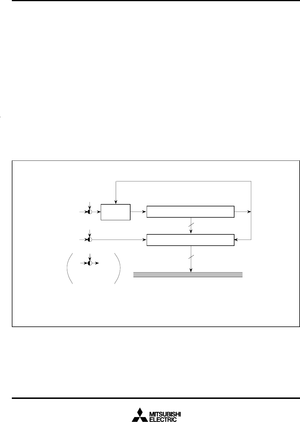
8
Data bus
Control
circuit
Connected to
black colored
side at rest.
Selection gate :
(Address 00D7
16
)
32µs
RE1
16µs
8-bit binary up counter (8)
Interrupt interval determination register (8)
RE0
8
INT1 (Note)
RE2
INT2 (Note)
Note: The pulse width of external interrupt INT1 and INT2 needs 5 or more machine cycles.
RE : Interrupt interval determination control register
PREVIOUS1718192021222324252627282930NEXT