MITSUBISHI MICROCOMPUTERS
M37207MF-XXXSP/FP, M37207M8-XXXSP
M37207EFSP/FP
SINGLE-CHIP 8-BIT CMOS MICROCOMPUTER for VOLTAGE SYNTHESIZER
and ON-SCREEN DISPLAY CONTROLLER
69
Fig. 65. Port Control Register
(11) CRT Output Pin Control
The CRT output pins R, G, B, I and OUT can also function as ports
P52, P53, P54, P55 and P56. Set the corresponding bit of the port P5
control register (address 00CB16) to “0” to specify these pins as CRT
output pins, or set it to “1” to specify it as a general-purpose port P5
pins.
The input polarity of signals HSYNC and VSYNC and output polarity of
signals R, G, B, I and OUT can be specified with the bits of the CRT
port control register (address 00EC16). Set a bit to “0” to specify posi-
tive polarity; set it to “1” to specify negative polarity.
The CRT clock I/O pins OSC1, OSC2 are controlled with the port
control register (address 020616).
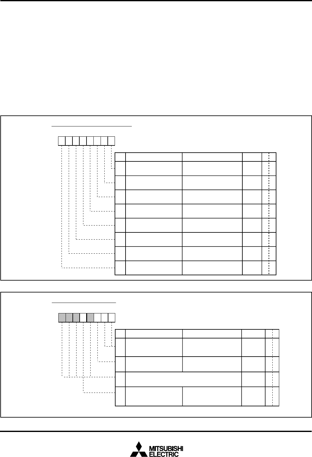
The CRT port control register is shown in Figure 64.
The port control register is shown in Figure 65.
Fig. 64. CRT Port Control Register
b7 b6 b5 b4 b3 b2 b1 b0
CRT port control register (CRTP) [Address 00EC
16
]
B Name Functions
After reset
R
W
CRT Port Control Register
0H
SYNC
input polarity
switch bit (HSYC)
0 : Positive polarity
1 : Negative polarity
0
1
0 : Positive polarity
1 : Negative polarity
0
2 R, G, B output polarity
switch bit (R/G/B)
0 : Positive polarity
1 : Negative polarity
0
3 I output polarity switch bit
(I)
0 : Positive polarity
1 : Negative polarity
0
4 OUT output polarity
switch bit (OUT)
0 : Positive polarity
1 : Negative polarity
0
5 R signal output switch bit
(R)
0 : R signal output
1 : MUTE signal output
0
6 G signal output switch bit
(G)
0 : G signal output
1 : MUTE signal output
0
7 B signal output switch bit
(B)
0 : B signal output
1 : MUTE signal output
0
V
SYNC
input polarity
switch bit (VSYC)
RW
RW
RW
RW
RW
RW
RW
RW
b7 b6 b5 b4 b3 b2 b1 b0
Port control register (P7D) [Address 0206
16
]
B Name Functions
After reset
R
W
Port Control Register
0, 1 Port P7 data input bits
(P7D0, P7D1)
When only OP1 = “0” and
OP0 = ”1,” input data is
valid. (See note)
Indeterminate
2
D-A/AD3 function selection
bit (P7D2)
0
RW
RW
0
Nothing is assigned. These bits are write disable bits.
When these bits are read out, the values are indeterminate.
R—
4P4
0
/X
CIN
, P4
1
/X
COUT
function selection bit
(P7D4)
0 : P4
0
, P4
1
1 : X
CIN
, X
COUT
0
RW
Note: OP is the CRT clock selection register.
0: AD3
1: D-A
3,
5 to 7


