TS2596
3A / 150KHz Buck Dc-Dc Converter
4/9
Version: E13
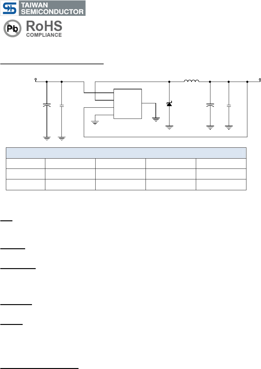
Typical Application Circuit (Continue)
2. Fixed Output Voltage Version
C2
0.1uF
D1
B340A
L1
47uH
1 2
C3
470uF
C1
470uF
U1
1
2
3
4
5
Vcc
SW
FB
EN
Vss
Vout=5.0V/3AVIN=24V
C6
0.1uF
L1 recommend value (I
OUT
=3A,)
V
OUT
2.5V 3.3V 5V 12V
V
IN
=12V 33uH 33uH 33~47uH NA
V
IN
=24V 33uH 33uH 47uH 68uH
Pin Function Description
Vcc
This is the positive input supply for the IC switching regulator. A suitable input bypass capacitor must be presented
at this pin to minimize voltage transients and to supply the switching currents needed by the regulator.
Ground
Circuit ground
SW Output
Internal switch. The voltage at this pin switches between (+Vcc – Vsat) and approximately – 0.5V, with a duty cycle
of approximately Vout / Vcc. To minimize coupling to sensitive circuitry, the PC board copper area connected to this
pin should be minimized.
Feedback
Sense the regulated output voltage to complete the feedback loop.
Enable
Allows the switching regulator circuit to be shutdown using logic level signals thus dropping the total input supply
current to approximately 100uA. Pulling this pin below a threshold voltage of approximately 1.3V turns the regulator
on, and pulling this pin above 1.3V (up to a maximum of Vcc) shuts the regulator down. If this shutdown feature is
not needed, the EN pin can be wired to the ground pin.
Thermal Considerations
The TS2596 is available in two packages, a TO-220-5L and TO-263-5L.
The TO-220-5L package needs a heat sink under most conditions. The size of the heat sink depends on the input
voltage, the output voltage, the load current and the ambient temperature. The TS2596 junction temperature rises
above ambient temperature for a 3A load and different input and output voltages. The data for these curves was
taken with the TS2596 (TO-220-5L package) operating as a buck switching regulator in an ambient temperature of
25
o
C (still air). These temperature rise numbers are all approximate and there are many factors that can affect
these temperatures. Higher ambient temperatures require more heat sinking.
The TO-263-5L surface mount package tab is designed to be soldered to the copper on a printed circuit board. The
copper and the board are the heat sink for this package and the other heat producing components, such as the
catch diode and inductor. The PC board copper area that the package is soldered to should be at least 0.8 in
2
, and
ideally should have 2 or more square inches of 2 oz. Additional copper area improves the thermal characteristics,


