Freelance Electronics Components Distributor
Closed Dec 25th-26th
800-300-1968
We Stock Hard to Find Parts

CM550

Part # CM550
Description 1%5W
Category RESISTOR
Availability In Stock
Qty 3
Manufacturer Available Qty
Clarostat
Date Code: 9526
  • Shipping Freelance Stock: 3
    Ships Immediately
Request For Quote


Technical Document


DISCLAIMER: The information provided herein is solely for informational purposes. Customers must be aware of the suitability of this product for their application, and consider that variable factors such as Manufacturer, Product Category, Date Codes, Pictures and Descriptions may differ from available inventory.

TS2596
3A / 150KHz Buck Dc-Dc Converter
1/9
Version: E13
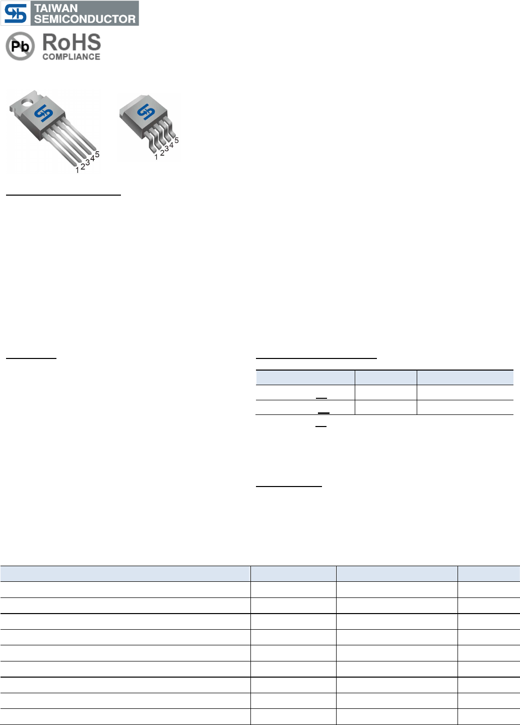
TO
-
220
-
5L
-
263
-
5L
(D
2
PAK)
General Description
The TS2596 Series are step-down switching regulators with all required active functions. It is capable of driving
3A load with excellent line and load regulations. These devices are available in fixed output voltages of 3.3V, 5V,
and an adjustable output version.
The TS2596 series operates at a switching frequency of 150kHz thus allowing smaller sized filter components
than what would be needed with lower frequency switching regulators. It substantially not only reduces the area of
board size but also the size of heat sink, and in some cases no heat sink is required. The ±4% tolerance on output
voltage within specified input voltages and output load conditions is guaranteed. Also, the oscillator frequency
accuracy is within ±10%. External shutdown is included. Featuring 100µA (typical) standby current. The output
switch includes cycle-by-cycle current limiting, as well as thermal shutdown for full protection under fault
conditions.
Features
Output Voltage: 3.3V, 5V & Adjustable version
Adjustable Output Voltage Range 1.23V~38.5V
150KHz fixed switching frequency
Voltage Mode Non-synchronous PWM control
Thermal Shutdown and Current Limit Protection
ON/OFF Shutdown Control Input
High Efficiency
Short Circuit Protect (SCP)
Operating Voltage Can be up to 40V
Output Load Current 3A
Low Power Standby Mode
Built-in switching transistor on chip
Ordering Information
Part No. Package
Packing
TS2596CZ5xx C0 TO-220-5L
50pcs / Tube
TS2596CM5xx RN
TO-263-5L
800pcs / 13” Reel
Note: Where xx denotes voltage option, available are
50= 5.0V
33= 3.3V
Leave blank for adjustable version
Application
Simple High-efficiency Step down Regulator
On-Card Switching Regulators
Positive to Negative Converter
Absolute Maximum Rating
Parameter Symbol Limit Unit
Maximum Supply Voltage V
CC
+45 V
Recommend Operating Supply Voltage V
OP
+4.5 to +40 V
SW, EN Pin Input Voltage V
SW
, V
EN
-0.3 to +40 V
Feedback Pin Voltage V
FB
-0.3 to +12 V
Power Dissipation P
D
Internally Limited W
Output Voltage to Ground V
OUT
-1 V
Storage Temperature Range T
ST
-65 to +150
o
C
Operating Temperature Range T
OP
-40 to +125
o
C
ESD Susceptibility (HBM) 2 kV
Pin
Definition
:
1. Input
2. SW Output
3. Ground
4. Feedback
5. Enable
TS2596
3A / 150KHz Buck Dc-Dc Converter
2/9
Version: E13
Thermal Information
Parameter Symbol Maximum Unit
Thermal Resistance* (Junction to Case)
TO-220-5L
Ө
JC
2
o
C/W
TO-263-5L
2
Thermal Resistance* (Junction to Ambient)
TO-220-5L
Ө
JA
50
o
C/W
TO-263-5L
50
Note: Ө
JA
is measured with the PCB copper area (need connect to GROUND pins) of approximately 1.5 in
2
(Multi-
layer)
Electrical Specifications (All Output Voltage Version)
(Ta = 25
o
C unless otherwise noted, V
IN
=12V for 3.3V, 5V, Adjustable version. I
LOAD
=0.3A)
Parameter Symbol
Test Condition Min
Typ
Max
Unit
Output Feedback
ADJ
V
FB
4.5V V
IN
40V
0.2A I
LOAD
3A
1.180
1.23
1.280
V
Efficiency η V
IN
=12V, I
LOAD
=3A, V
OUT
=5V -- 77 -- %
Output Feedback
3.3V
V
FB
4.75V V
IN
40V
0.2A I
LOAD
3A
3.135
3.3V
3.465
V
Efficiency η V
IN
=12V, I
LOAD
=3A -- 75 -- %
Output Feedback
5V
V
FB
7V V
IN
40V
0.2A I
LOAD
3A
4.75
5 5.25
V
Efficiency η V
IN
=12V, I
LOAD
=3A -- 80 -- %
Feedback Bias Current I
FB
V
FB
=1.3V (Adj version only) -- 10 100 nA
Oscillator Frequency F
OSC
127 150 173 KHz
Soft-Start Time T
SS
Rising edge of EN on to I
CL
-- 3 -- mS
Current Limit I
CL
Pear Current, no outside circuit
V
FB
=0V force driver on
3.3 -- -- A
Oscillator Frequency of Short Circu
it
Protect
F
SCP
When current limit occurred and
V
FB
<0.5V, Ta = 25
o
C
110 150 173 KHz
Saturation Voltage V
SAT
I
OUT
=3A, No outside circuit
V
FB
=0V force driver on
-- 1.15
1.50
V
ON/OFF Pin Logic Input Threshold
Voltage
V
IL
Low (regulator ON) --
1.3
0.6
V
V
IH
High (regulator OFF) 2.0 --
ON/OFF Pin Logic Input Current
I
H
V
LOGIC
=2.5V (OFF) -- 5 15
µA
I
L
V
LOGIC
=0.5V (ON) -- 0.02
5
Maximum Duty Cycle (ON)
DC
V
FB
=0V force driver on -- 100 --
%
Maximum Duty Cycle (OFF) V
FB
=12V force driver off -- 0 --
Quiescent Current I
Q
V
FB
=12V force driver off -- 5 10 mA
Standby Quiescent Current I
STBY
ON/OFF pin=5V --
80
200
µA
V
IN
=40V 250
SW Pin Leakage
Current
SW pin = 0
I
SWL
No outside circuit,
V
FB
=12V force driver off
-- 0.3 2 mA
SW pin = -1 V
IN
=12V -- 7.5 30 mA
TS2596
3A / 150KHz Buck Dc-Dc Converter
3/9
Version: E13
Block Diagram
Typical Application Circuit
1. Adjustable Output Voltage Version
VIN=12V
C2
0.1uF
D1
B340A
L1
33uH
1 2
C3
470uF
C1
470uF
U1
1
2
3
4
5
Vcc
SW
FB
EN
Vss
Vout=5.0V/3AVIN=12V
ON/OFF
C6
0.1uF
R2
1.5K
R1
4.7K
VIN=24V
C2
0.1uF
D1
B340A
L1
47uH
1 2
C3
470uF
C1
470uF
U1
1
2
3
4
5
Vcc
SW
FB
EN
Vss
Vout=5.0V/3AVIN=24V
C6
0.1uF
R2
1.5K
R1
4.7K
V
OUT
= V
FB
×
(1 +
R2
R1
), V
FB
= 1.23V, R2 = 0.7K ~ 3K
V
OUT
R2 R1
5.0V 1.5K 4.7K
3.3V 1.5K 2.5K
2.5V 1.5K 1.5K
123NEXT