August 2005 5 M9999-082605-B
LM2576 Micrel, Inc.
Electrical Characteristics (continued)
LM2576 Units
Symbol Parameter Conditions Typ Limit (Limits)
(Note 2)
ON/OFF CONTROL, FIXED and ADJUSTABLE REGULATORS Test Circuit
Figure 1
V
IH
ON/OFF Pin Logic V
OUT
= 0V 1.4 2.2/2.4 V(min)
V
IL
Input Level V
OUT
= 5V 1.2 1.0/0.8 V(max)
I
IH
ON /OFF Pin Logic ON /OFF Pin = 5V (OFF) 4 µA
Current 30 µA(max)
I
IL
ON/OFF Pin = 0V (ON) 0.01 µA
10 µA(max)
Note 1: Absolute Maximum Rating indicate limits beyond which damage to the device may occur. Operating Ratings indicate conditions for which the device
is intended to be functional, but do not guarantee specific performance limits. For guaranteed specifications and test conditions, see the Electrical
Characteristics.
Note 2: All limits guaranteed at room temperature (standard type face) and at temperature extremes (bold type face) . All room temperature limits are
100% production tested. All limits at temperature extreme are guaranteed via testing.
Note 3: External components such as the catch diode, inductor, input and output capacitors can affect switching regulator system performance. When the
LM2576/LM1576 is used as shown in
Figure 1
test circuit, system performance will be shown in system parameters section of Electrical
Characteristics.
Note 4: Output (pin 2) sourcing current. No diode, inductor or capacitor connected to output.
Note 5: Feedback (pin 4) removed from output and connected to 0V.
Note 6: Feedback (pin 4) removed from output and connected to 12V to force the output transistor OFF.
Note 7: Junction to ambient thermal resistance (no external heat sink) for the 5-lead TO-220 package mounted vertically, with 1/2" leads in a socket, or
on PC board with minimum copper area.
Note 8: Junction to ambient thermal resistance (no external heat sink) for the 5-lead TO-220 package mounted vertically, with 1/4" leads soldered to PC
board containing approximately 4 square inches of copper area surrounding the leads.
Note 9: Junction to ambient thermal resistance with approximately 1 square inch of pc board copper surrounding the leads. Additional copper will lower
thermal resistance further.
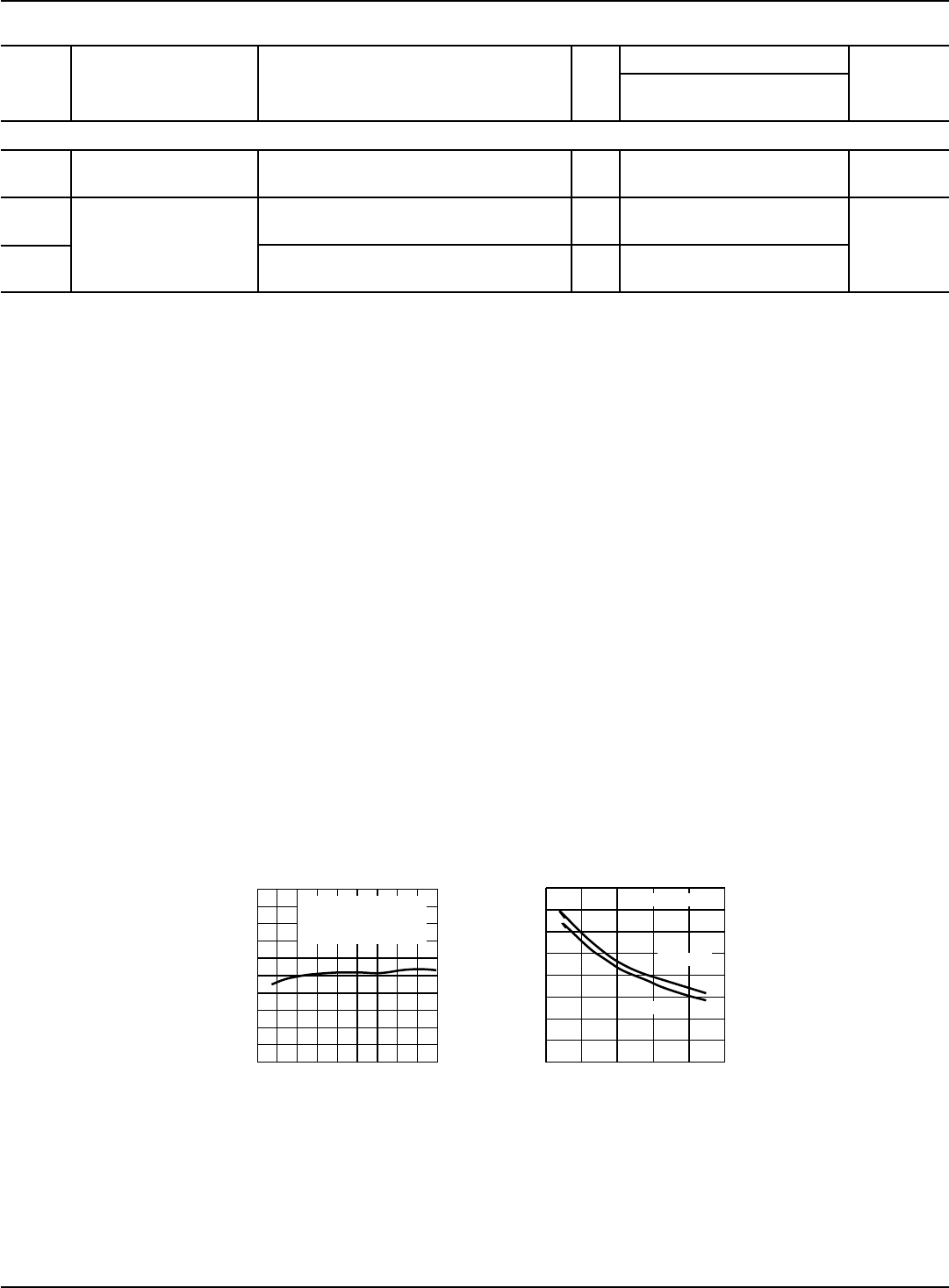
Typical Performance Characteristics
Normalized
Feedback Voltage*
JUNCTION TEMPERATURE (˚C)
NORMALIZED FEEDBACK VOLTAGE (mV)
25
20
15
10
5
0
-5
-10
-15
-20
-25
-75 -50 -25 0 25 50 75 100125150
V
IN
= 12V
I
LOAD
= 200mA
Normalized to T
J
= 25˚C
Feedback Voltage
vs Duty Cycle*
DUTY CYCLE (%)
FEEDBACK VOLTAGE CHANGE (mV)
20
15
10
5
0
-5
-10
-15
-20
ILOAD = 200 mA
VIN = 40V
VIN = 7V
0 20 40 60 80 100
* Adjustable version only


