Closed Dec 25th-26th
800-300-1968
We Stock Hard to Find Parts
My Account
|
My Orders
|
My Cart
Questions?
(800) 300-1968
Register
(current)
My Account
(current)
My Orders
(current)
My Cart
(current)
Categories
(current)
Manufacturers
Request a Quote
Sell Your Excess
Consignment
Quality Assurance
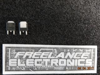
MC79M15BT
Part #
MC79M15BT
Description
IC REG LDO -15V 0.5A TO220AB
Category
RECTIFIER
Availability
In Stock
Qty
6
Qty
Price
1 +
$2.26338
Manufacturer
Available
Qty
Motorola Corp
Date Code: 9734
Freelance Stock:
6
Ships Immediately
Add to Cart
Related Items
ON Semiconductor
RECTIFIER
MC79M05BDTG
$0.15748
Motorola Corp
RECTIFIER
MC79M05CT
$0.14569
ON Semiconductor
IC
MC79M05BDT
$0.54244
Motorola Corp
IC
MC79M05CDT
$0.30134
International Rectifier
RECTIFIER
10BQ060
$0.28930
International Rectifier
RECTIFIER
10CTQ150S
$2.10035