Closed Dec 25th-26th
800-300-1968
We Stock Hard to Find Parts
My Account
|
My Orders
|
My Cart
Questions?
(800) 300-1968
Register
(current)
My Account
(current)
My Orders
(current)
My Cart
(current)
Categories
(current)
Manufacturers
Request a Quote
Sell Your Excess
Consignment
Quality Assurance
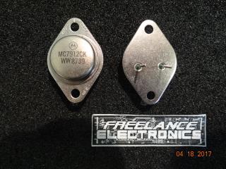
MC7912BT
Part #
MC7912BT
Description
IC REG LDO -12V 1A TO220AB
Category
RECTIFIER
Availability
In Stock
Qty
6
Qty
Price
1 +
$0.80361
Manufacturer
Available
Qty
Motorola Corp
Freelance Stock:
6
Ships Immediately
Add to Cart
Related Items
Fairchild Semiconductor
RECTIFIER
MC7912C
$6.32354
ON Semiconductor
RECTIFIER
MC7912CT
$0.76400
Motorola Corp
RECTIFIER
MC7915CTIQ
ON Semiconductor
REGULATOR
MC7912ACT
$0.35615
ON Semiconductor
IC
MC7912CD2T
$0.21016
Motorola Corp
VOLTAGE REGULAT
MC7912CK
$15.74171