Closed Dec 25th-26th
800-300-1968
We Stock Hard to Find Parts
My Account
|
My Orders
|
My Cart
Questions?
(800) 300-1968
Register
(current)
My Account
(current)
My Orders
(current)
My Cart
(current)
Categories
(current)
Manufacturers
Request a Quote
Sell Your Excess
Consignment
Quality Assurance
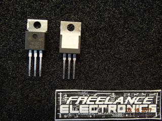
MC7815CTG
Part #
MC7815CTG
Description
LDO Regulator Pos 15V 1A 3-Pin(3+Tab) TO-220 Rail
Category
RECTIFIER
Availability
Out of Stock
Qty
0
Qty
Price
1 +
$0.11374
Related Items
ON Semiconductor
RECTIFIER
MC7812ACT
$1.52063
Motorola Corp
RECTIFIER
MC7812BT
$0.35615
Motorola Corp
RECTIFIER
MC7815CD2T
$1.59155
ON Semiconductor
RECTIFIER
MC7815CT
$0.77678
Motorola Corp
VOLTAGE REGULAT
MC7812CK
$23.02385
Motorola Corp
TRANSISTOR
MC7812CT
$0.30134