9
This product has not been designed or tested for use in, and is not intended for use in, applications implanted into the human body
nor in applications in which failure of the product could lead to death, personal injury or property damage, including but not limited
to equipment used in the operation of nuclear facilities, life-support machines, cardiac debrillators or similar emergency medical
equipment, aircraft navigation or communication or control systems, air trafc control systems, or weapons systems.
Copyright © 2013 Cree, Inc. All rights reserved. The information in this document is subject to change without notice. Cree and the
Cree logo are registered trademarks and Z-REC and Z-FET are trademarks of Cree, Inc.
9 C2M0160120D Rev.
-
Cree, Inc.
4600 Silicon Drive
Durham, NC 27703
USA Tel: +1.919.313.5300
Fax: +1.919.313.5451
www.cree.com/power
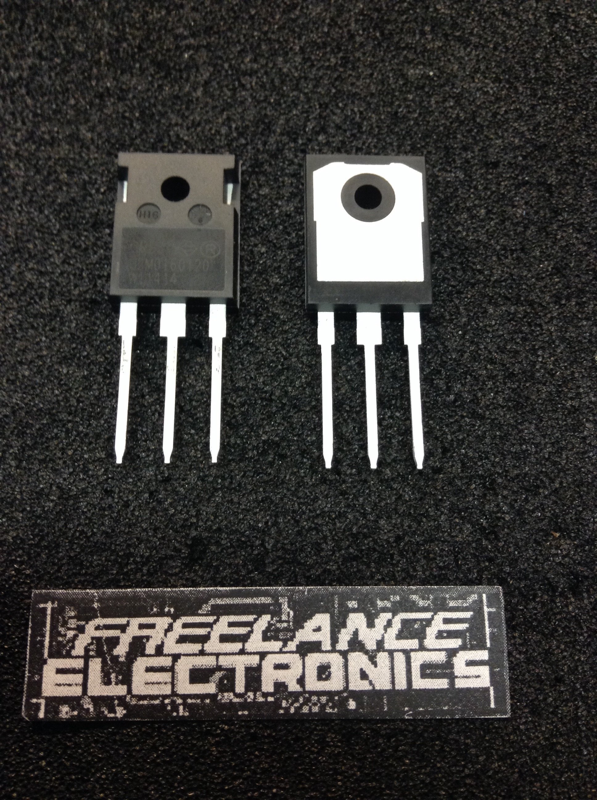
Package Dimensions
Package TO-247-3
Recommended Solder Pad Layout
TO-247-3
(1)
(2)
(3)
POS
Inches Millimeters
Min Max Min Max
A .190 .205 4.83 5.21
A1 .090 .100 2.29 2.54
A2 .075 .085 1.91 2.16
b .042 .052 1.07 1.33
b1 .075 .095 1.91 2.41
b2 .075 .085 1.91 2.16
b3 .113 .133 2.87 3.38
b4 .113 .123 2.87 3.13
c .022 .027 0.55 0.68
D .819 .831 20.80 21.10
D1 .640 .695 16.25 17.65
D2 .037 .049 0.95 1.25
E .620 .635 15.75 16.13
E1 .516 .557 13.10 14.15
E2 .145 .201 3.68 5.10
E3 .039 .075 1.00 1.90
E4 .487 .529 12.38 13.43
e .214 BSC 5.44 BSC
N 3 3
L .780 .800 19.81 20.32
L1 .161 .173 4.10 4.40
ØP .138 .144 3.51 3.65
Q .216 .236 5.49 6.00
S .238 .248 6.04 6.30
Part Number Package Marking
C2M0160120D TO-247-3 C2M0160120