Closed Dec 25th-26th
800-300-1968
We Stock Hard to Find Parts
My Account
|
My Orders
|
My Cart
Questions?
(800) 300-1968
Register
(current)
My Account
(current)
My Orders
(current)
My Cart
(current)
Categories
(current)
Manufacturers
Request a Quote
Sell Your Excess
Consignment
Quality Assurance
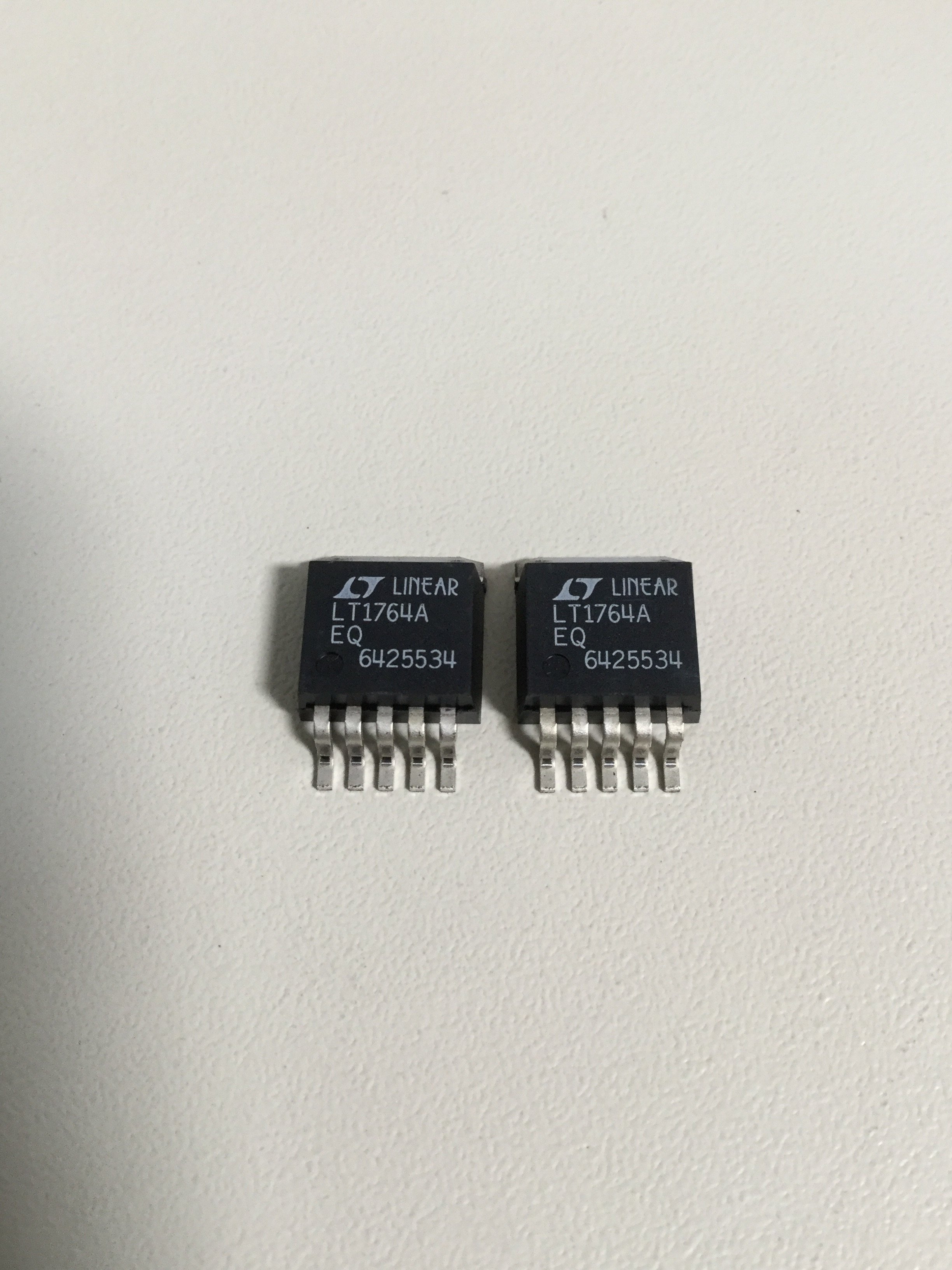
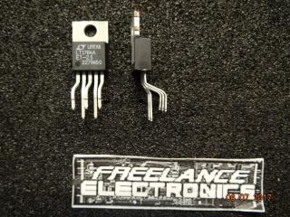
LT1764AEQ
Part #
LT1764AEQ
Description
LDO Regulator Pos 1.21V to 20V 3A 6-Pin(5+Tab) DDPAK
Category
RECTIFIER
Availability
Out of Stock
Qty
0
Qty
Price
1 +
$8.29823
Related Items
Linear Technology
RECTIFIER
LT1764AEQ-2.5
$10.45429
Linear Technology
RECTIFIER
LT1764AET-2.5
$3.23197
Linear Technology
RECTIFIER
LT1764EQ
$12.17610
Linear Technology
RECTIFIER
LT1764ET-2.5
$10.23564
Linear Technology
IC
LT1761ES5-1.5#TRMPBF
$1.30556
Linear Technology
IC
LT1761ES5-1.8#TRPBF
$2.06125