Freelance Electronics Components Distributor
Closed Dec 25th-26th
800-300-1968
We Stock Hard to Find Parts

LM340AT-5.0

Part # LM340AT-5.0
Description SERIES 3-TERMINAL POSITIVE REGULATORS - Rail/Tube
Category RECTIFIER
Availability Out of Stock
Qty 0
Qty Price
1 + $0.74110


Technical Document


DISCLAIMER: The information provided herein is solely for informational purposes. Customers must be aware of the suitability of this product for their application, and consider that variable factors such as Manufacturer, Product Category, Date Codes, Pictures and Descriptions may differ from available inventory.

SEMICONDUCTOR
TECHNICAL DATA
THREE–TERMINAL
POSITIVE FIXED
VOLTAGE REGULATORS
Order this document by LM340/D
Pin 1. Input
2. Ground
3. Output
T SUFFIX
PLASTIC PACKAGE
CASE 221A
Heatsink surface is connected to Pin 2.
3
1
2
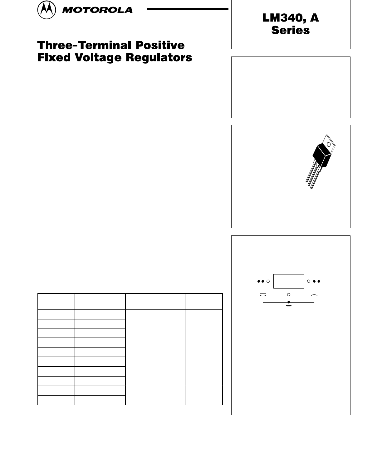
Simplified Application
A common ground is required between the input and
the output voltages. The input voltage must remain
typically 1.7 V above the output voltage even during
the low point on the input ripple voltage.
XX these two digits of the type number indicate
voltage.
*C
in
is required if regulator is located an
appreciable distance from power supply filter.
** C
O
is not needed for stability; however, it does
improve transient response. If needed, use a
0.1 µF ceramic disc.
LM340–XX
Input
C
in
*
0.33
µ
F
C
O
**
Output
1
MOTOROLA ANALOG IC DEVICE DATA
This family of fixed voltage regulators are monolithic integrated circuits
capable of driving loads in excess of 1.0 A. These three–terminal regulators
employ internal current limiting, thermal shutdown, and safe–area
compensation. Devices are available with improved specifications, including
a 2% output voltage tolerance, on A–suffix 5.0, 12 and 15 V device types.
Although designed primarily as a fixed voltage regulator, these devices
can be used with external components to obtain adjustable voltages and
currents. This series of devices can be used with a series–pass transistor to
boost output current capability at the nominal output voltage.
Output Current in Excess of 1.0 A
No External Components Required
Output Voltage Offered in 2% and 4% Tolerance*
Internal Thermal Overload Protection
Internal Short Circuit Current Limiting
Output Transistor Safe–Area Compensation
ORDERING INFORMATION
Device
Output Voltage
and Tolerance
Operating
Temperature Range
Package
LM340T–5.0 5.0 V ± 4%
T 0 12 C
Pl i P
LM340AT–5.0 5.0 V ± 2%
T 0 12 C
Pl i P
LM340T–6.0 6.0 V ± 4%
T 0 12 C
Pl i P
LM340T–8.0 8.0 V ± 4%
T 0 12 C
Pl i P
LM340T–12 12 V ± 4%
T
J
=0
°
to +125
°
C
Plastic Power
LM340AT–12 12 V ± 2%
T
J
=
0°
t
o +
125°C
Pl
as
ti
c
P
ower
LM340T–15 15 V ± 4%
LM340AT–15 15 V ± 2%
LM340T–18 18 V ± 4%
LM340T–24 24 V ± 4%
* 2% regulators are available in 5, 12 and 15 V devices.
Motorola, Inc. 1996 Rev 1
LM340, A Series
2
MOTOROLA ANALOG IC DEVICE DATA
MAXIMUM RATINGS
(T
A
= +25°C unless otherwise noted.)
Rating Symbol Value Unit
Input Voltage (5.0 V – 18 V)
Input Voltage (24 V)
V
in
35
40
Vdc
Power Dissipation and Thermal Characteristics
Plastic Package
T
A
= +25°C
Derate above T
A
= +25°C
Thermal Resistance, Junction–to–Air
T
C
= +25°C
Derate above T
C
= +75°C (See Figure 1)
Thermal Resistance, Junction–to–Case
P
D
1/
θJA
θ
JA
P
D
1/
θJA
θ
JC
Internally Limited
15.4
65
Internally Limited
200
5.0
W
mW/°C
°C/W
W
mW/°C
°C/W
Storage Temperature Range T
stg
–65 to +150 °C
Operating Junction Temperature Range T
J
0 to +150 °C
Representative Schematic Diagram
1.0k
210
Input
16k
6.7V
300
1.0k
100
200
3.6k
6.4k
520
3.0k
5.6k
10pF
300
13
0.12
Output
200
50
2.6k
6.0k
40
pF
Gnd
2.8k
3.9k2.0k
6.0k
1.0k
LM340, A Series
3
MOTOROLA ANALOG IC DEVICE DATA
LM340–5.0
ELECTRICAL CHARACTERISTICS
(V
in
= 10 V, I
O
= 500 mA, T
J
= T
low
to T
high
[Note 1], unless otherwise noted.)
Characteristics
Symbol Min Typ Max Unit
Output Voltage (T
J
= +25°C)
I
O
= 5.0 mA to 1.0 A
V
O
4.8 5.0 5.2 Vdc
Line Regulation (Note 2)
8.0 Vdc to 20 Vdc
7.0 Vdc to 25 Vdc (T
J
= +25°C)
8.0 Vdc to 12 Vdc, I
O
= 1.0 A
7.3 Vdc to 20 Vdc, I
O
= 1.0 A (T
J
= +25°C)
Reg
line
50
50
25
50
mV
Load Regulation (Note 2)
5.0 mA I
O
1.0 A
5.0 mA I
O
1.5 A (T
J
= +25°C)
250 mA I
O
750 mA (T
J
= +25°C)
Reg
load
50
50
25
mV
Output Voltage
7.0 V
in
20 Vdc, 5.0 mA I
O
1.0 A, P
D
15 W
V
O
4.75 5.25 Vdc
Quiescent Current
I
O
= 1.0 A
T
J
= +25°C
I
B
4.0
8.5
8.0
mA
Quiescent Current Change
7.0 V
in
25 Vdc, I
O
= 500 mA
5.0 mA I
O
1.0 A, V
in
= 10 V
7.5 V
in
20 Vdc, I
O
= 1.0 A
I
B
1.0
0.5
1.0
mA
Ripple Rejection
I
O
= 1.0 A (T
J
= +25°C)
RR 62 80 dB
Dropout Voltage V
I
– V
O
1.7 Vdc
Output Resistance (f = 1.0 kHz) r
O
2.0 m
Short Circuit Current Limit (T
J
= +25°C) I
SC
2.0 A
Output Noise Voltage (T
A
= +25°C)
10 Hz f 100 kHz
V
n
40 µV
Average Temperature Coefficient of Output Voltage
I
O
= 5.0 mA
TCV
O
±0.6 mV/°C
Peak Output Current (T
J
= +25°C) I
O
2.4 A
Input Voltage to Maintain Line Regulation (T
J
= +25°C)
I
O
= 1.0 A
7.3 Vdc
NOTES: 1. T
low
to T
high
= 0° to +125°C
2. Load and line regulation are specified at constant junction temperature. Changes in V
O
due to heating effects must be taken into account separately.
Pulse testing with low duty cycle is used.
DEFINITIONS
Line Regulation – The change in output voltage for a
change in the input voltage. The measurement is made
under conditions of low dissipation or by using pulse
techniques such that the average chip temperature is not
significantly affected.
Load Regulation – The change in output voltage for a
change in load current at constant chip temperature.
Maximum Power Dissipation – The maximum total device
dissipation for which the regulator will operate within
specifications.
Quiescent Current – That part of the input current that is not
delivered to the load.
Output Noise Voltage – The rms AC voltage at the output,
with constant load and no input ripple, measured over a
specified frequency range.
1234567NEXT