Closed Dec 25th-26th
800-300-1968
We Stock Hard to Find Parts
My Account
|
My Orders
|
My Cart
Questions?
(800) 300-1968
Register
(current)
My Account
(current)
My Orders
(current)
My Cart
(current)
Categories
(current)
Manufacturers
Request a Quote
Sell Your Excess
Consignment
Quality Assurance
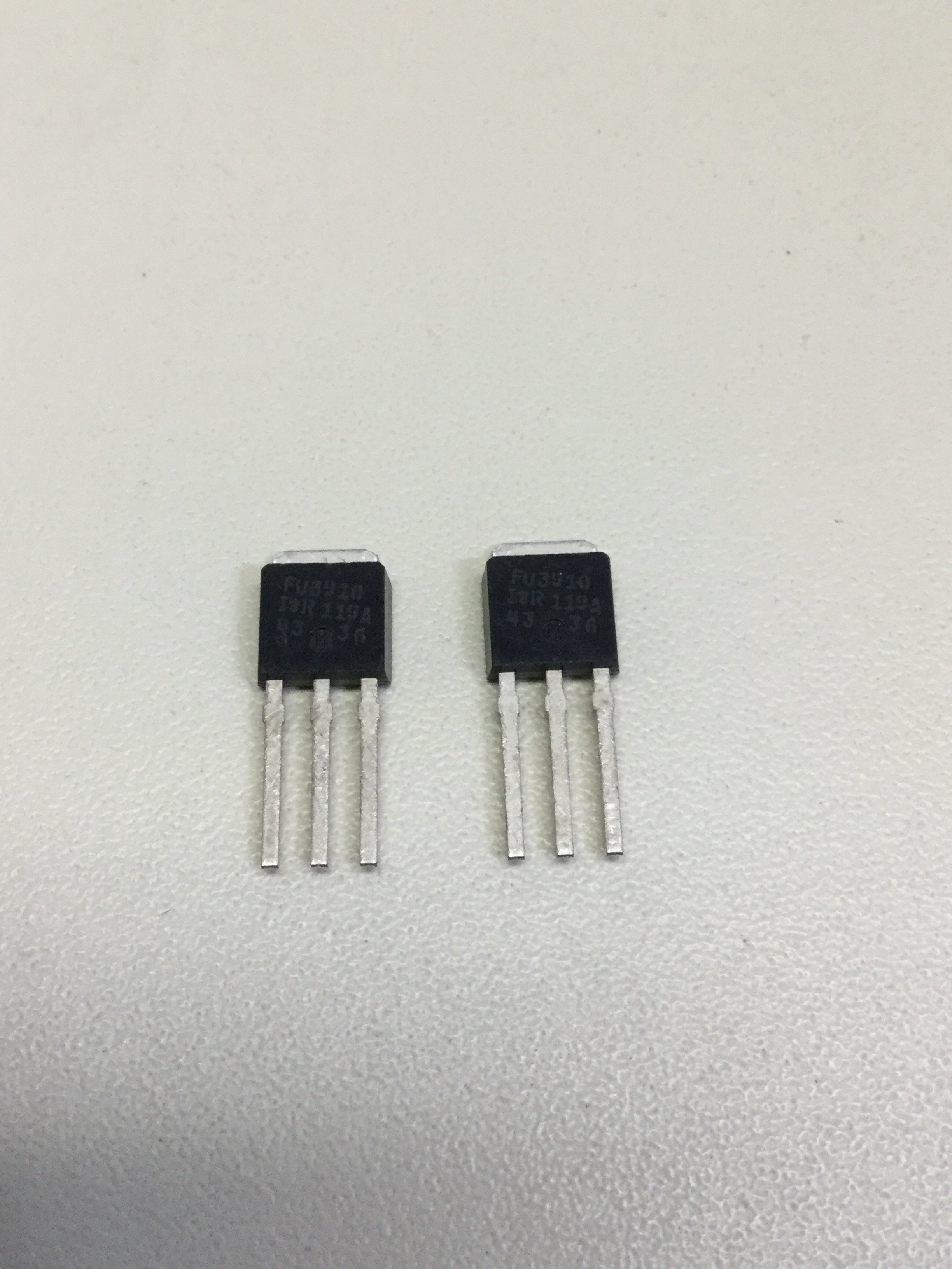
IRFU3910
Part #
IRFU3910
Description
MOSFET N-CH 100V 16A I-PAK
Category
RECTIFIER
Availability
In Stock
Qty
19
Qty
Price
1 - 3
$15.02217
4 - 7
$11.94945
8 - 11
$11.26663
12 - 15
$10.47000
16 +
$9.33195
Manufacturer
Available
Qty
International Rectifier
Date Code: 0119
Freelance Stock:
19
Ships Immediately
Add to Cart
Related Items
International Rectifier
RECTIFIER
10BQ060
$0.28930
International Rectifier
RECTIFIER
10CTQ150S
$2.10035
International Rectifier
RECTIFIER
10MQ060NTRPBF
$0.42140
International Rectifier
RECTIFIER
10TQ045
$0.75375
Solitron
TRANSISTOR
12272080
$45.50319
Generic
RECTIFIER
12CT0045