Closed Dec 25th-26th
800-300-1968
We Stock Hard to Find Parts
My Account
|
My Orders
|
My Cart
Questions?
(800) 300-1968
Register
(current)
My Account
(current)
My Orders
(current)
My Cart
(current)
Categories
(current)
Manufacturers
Request a Quote
Sell Your Excess
Consignment
Quality Assurance
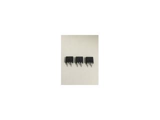
IRFS38N20DTRLP
Part #
IRFS38N20DTRLP
Description
MOSFET, 200V, 44A, 54 MOHM, 60 NC QG, D2-PAK - Tape and Re
Category
RECTIFIER
Availability
Out of Stock
Qty
0
Qty
Price
1 +
$0.70609
Related Items
International Rectifier
RECTIFIER
IRFS31N20D
$0.87313
International Rectifier
RECTIFIER
IRFS31N20DPBF
$0.55599
International Rectifier
RECTIFIER
IRFS3206PBF
$1.94766
International Rectifier
RECTIFIER
10BQ060
$0.28930
International Rectifier
RECTIFIER
10CTQ150S
$2.10035
International Rectifier
RECTIFIER
10MQ060NTRPBF
$0.42140