Adjusting the Output Voltage of the PTV12020x Series
PTV12020W/L
SLTS231A – NOVEMBER 2004 – REVISED FEBRUARY 2005
APPLICATION INFORMATION (continued)
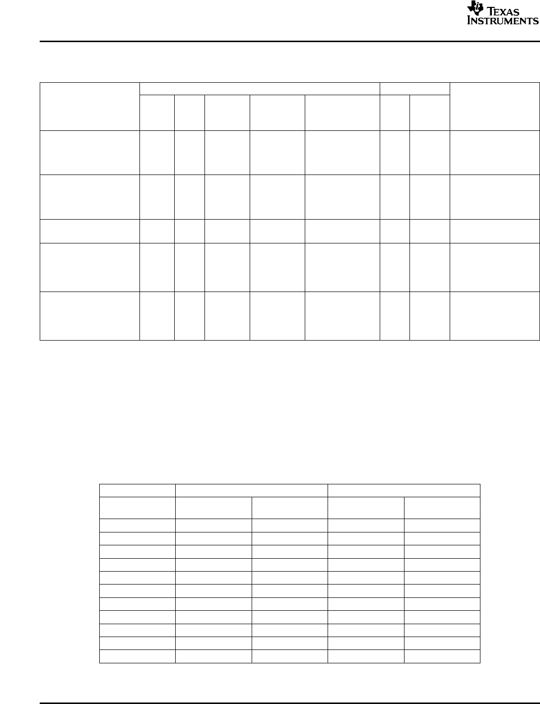
Table 1. Input/Output Capacitors (continued)
Capacitor Characteristics Quantity
Max Ripple
Capacitor Vendor, Vendor
Working Max ESR Optional
Value Current at Physical Size Input
Type/Series (Style) Part Number
Voltage at 100 kHz Output
(µF) 85 ° C (Irms) (mm) Bus
(V) ( Ω ) Bus
(mA)
T520, Poly-Tant 10 330 0.040 1800 N/R
(1)
≤ 5 T520X337M010AS
T530, Poly-Tant/Organic 10 330 0.010 >3800 N/R
(1)
≤ 1 T530X337M010ASE010
43 W × 7.3 L × 4 H
6.3 470 0.010 4200 N/R
(1)
≤ 1 T530X477M006ASE010
(V
O
≤ 5.1 V)
Vishay-Sprague
595D, Tantalum (SMD) 10 470 0.100 1440 7.2 L × 6 W × 4.1 H N/R
(1)
≤ 5 595D477X0010R2T
(V
O
≤ 5.1 V)
94SA, Os-Con (Radial) 16 1,000 0.015 9740 16 × 25 1 ≤ 2 94SA108X0016HBP
Kemet, Ceramic X5R (SMD) 16 10 0.002 — 3225 =>2
(3)
≤ 5 C1210C106M4PAC
6.3 47 0.002 3225 N/R
(1)
≤ 5 C1210C476K9PAC
Murata, Ceramic X5R (SMD) 6.3 100 0.002 — 3225 N/R
(1)
≤ 3 GRM32ER60J107M
6.3 47 3225 N/R
(1)
≤ 5 GRM32ER60J476M
16 22 =>1
(3)
≤ 5 GRM32ER61C226K
16 10 =>2
(3)
≤ 5 GRM32DR61C106K
TDK, Ceramic X5R (SMD) 6.3 100 0.002 — 3225 N/R
(1)
≤ 3 C3225X5R0J107MT
6.3 47 3225 N/R
(1)
≤ 5 C3225X5R0J476MT
16 22 =>1
(3)
≤ 5 C3225X5R1C226MT
16 10 =>2
(4)
≤ 5 C3225X5R1C106MT
(3) Ceramic capacitors are required to complement electrolytic types at the input and to reduce high-frequency ripple current.
(4) Ceramic capacitors are required to complement electrolytic types at the input and to reduce high-frequency ripple current.
The V
O
Adjust control (pin 8) sets the output voltage of the PTV12020 product. The adjustment range is from
1.2 V to 5.5 V for the W-suffix modules and 0.8 V to 1.8 V for L-suffix modules. The adjustment method requires
the addition of a single external resistor, R
SET
, that must be connected directly between the V
O
Adjust and GND
(pin 1 or 2). Table 2 gives the preferred value of the external resistor for a number of standard voltages, along
with the actual output voltage that this resistance value provides. Figure 11 shows the placement of the required
resistor.
Table 2. Standard Values of R
SET
for Common Output Voltages
PTV12020W PTV12020L
V
O
R
SET
V
O
R
SET
V
O
(Required) (Standard Value) (Actual) (Standard Value) (Actual)
5 V 280 Ω 5.009 V N/A N/A
3.3 V 2.0 k Ω 3.294 V N/A N/A
2.5 V 4.32 k Ω 2.503 V N/A N/A
2 V 8.06 k Ω 2.010 V N/A N/A
1.8 V 11.5 k Ω 1.801 V 130 Ω 1.800 V
1.5 V 24.3 k Ω 1.506 V 3.57 k Ω 1.499 V
1.2 V Open 1.200 V 12.1 k Ω 1.201 V
1.1 V N/A N/A 18.7 k Ω 1.101 V
1.0 V N/A N/A 32.4 k Ω 0.999 V
0.9 V N/A N/A 71.5 k Ω 0.901 V
0.8 V N/A N/A Open 0.800 V
10


