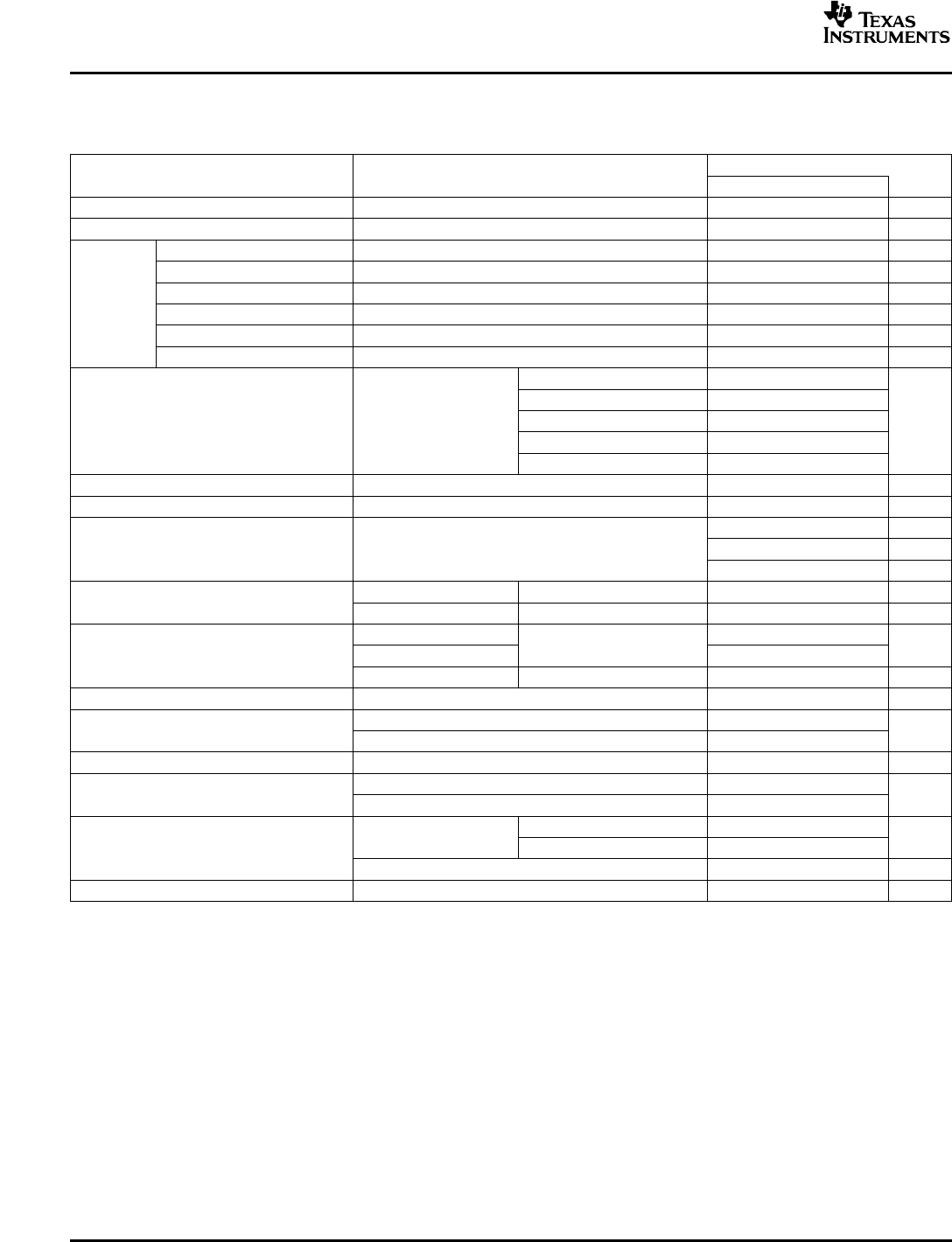
ELECTRICAL CHARACTERISTICS
PTV12020W/L
SLTS231A – NOVEMBER 2004 – REVISED FEBRUARY 2005
operating at 25 ° C free-air temperature, V
I
= 12 V, V
O
= 1.8 V, C1 = 560 µF, C2 = 22 µF, C3 = 0 µF, and I
O
= I
O
max (unless
otherwise noted)
PTV12020L
PARAMETER TEST CONDITIONS UNIT
MIN TYP MAX
I
O
Output current Natural convection airflow 0 16
(1)
A
V
I
Input voltage range Over I
O
load range 10.8 13.2 V
Set-point voltage tolerance ± 2%
(2)
Temperature variation –40 ° C <T
A
< 85 ° C ± 0.5%
Line regulation Over V
I
range ± 10 mV
V
O
Load regulation Over I
O
range ± 12 mV
Total output variation Includes set-point, line, load, –40 ° C ≤ T
A
≤ 85 ° C ± 3
(2)
%V
o
Adjust range Over V
I
range 0.8 1.8 V
R
SET
= 130 Ω , V
O
= 1.8 V 87%
R
SET
= 3.57 k Ω , V
O
= 1.5 V 85%
η Efficiency I
O
= I
O
max R
SET
= 12.1 k Ω , V
O
= 1.2 V 83%
R
SET
= 32.4 k Ω , V
O
= 1 V 80%
R
SET
= open cct., V
O
= 0.8 V 77%
Output voltage ripple (pk-pk) 20-MHz bandwidth 2 %V
O
I
O
(trip) Overcurrent threshold Reset, followed by auto-recovery 30 A
1-A/µs load step, 50 to 100% I
O
max, C3 = 330 µF
Transient response Recovery time 70 µs
V
o
over/undershoot 100 mV
I
IL
Input low current Pin to GND –0.13 mA
Track control (pin 9)
Control slew-rate limit C3 ≤ C3 (max) 1 V/ms
V
IH
Input high voltage 2 Open
(3)
Referenced to GND V
Inhibit control (pin 12) V
IL
Input low voltage –0.2 0.6
I
IL
Input low current Pin to GND –0.24 mA
I
I
(stby) Input standby current Inhibit (pin 12) to GND, Track (pin 9) open 10 mA
V
I
increasing 9.5 10.4
UVLO Undervoltage lockout V
V
I
decreasing 8.8 9
ƒ
S
Switching frequency Over V
I
and I
O
ranges 200 250 300 kHz
Nonceramic (C1) 560
(4)
External input capacitance µF
Ceramic (C2) 22
(4)
Nonceramic 0 330
(5)
6,600
(6)
Capacitance value µF
External output capacitance (C3) Ceramic 0 300
Equivalent series resistance (nonceramic) 4
(7)
m Ω
MTBF Reliability Per Telcordia SR-332, 50% stress, T
A
= 40 ° C, ground benign 4.9 10
6
Hrs
(1) See thermal derating curves for safe operating area (SOA), or consult factory for appropriate derating.
(2) The set-point voltage tolerance is affected by the tolerance and stability of R
SET
. The stated limit is unconditionally met if R
SET
has a
tolerance of 1%, with 100 ppm/ ° C or better temperature stability.
(3) This control pin is pulled up to an internal supply voltage. To avoid risk of damage to the module, do not apply an external voltage
greater than 7 V. If this input is left open-circuit, the module operates when input power is applied. A small low-leakage (<100 nA)
MOSFET is recommended for control. For further information, consult the related application note.
(4) A 22-µF high-frequency ceramic capacitor and 560-µF electrolytic input capacitor are required for proper operation. The electrolytic
capacitor must be rated for the minimum ripple current rating. Consult the Application Information for guidance on input capacitor
selection.
(5) An external output capacitor is not required for basic operation. Adding 330 µF of distributed capacitance at the load improves the
transient response.
(6) This is the calculated maximum. The minimum ESR limitation often results in a lower value. Consult the Application Informaiton for
further guidance.
(7) This is the typical ESR for all the electrolytic (nonceramic) output capacitance. Use 7 m Ω as the minimum when using max-ESR values
to calculate.
4


