Closed Dec 25th-26th
800-300-1968
We Stock Hard to Find Parts
My Account
|
My Orders
|
My Cart
Questions?
(800) 300-1968
Register
(current)
My Account
(current)
My Orders
(current)
My Cart
(current)
Categories
(current)
Manufacturers
Request a Quote
Sell Your Excess
Consignment
Quality Assurance
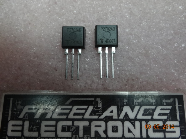
P2702AB
Part #
P2702AB
Description
SIDAC 2CHP 120/240V 250A TO-220
Category
MICROCIRCUITS
Availability
Out of Stock
Qty
0
Qty
Price
1 +
$0.88054
Related Items
HH Smith
MICROCIRCUITS
01-2603-4-0210
$10.85289
RPTRON
MICROCIRCUITS
023957
Rotron Incorporated
MICROCIRCUITS
033468
Rotron Incorporated
MICROCIRCUITS
034749
Rotron Incorporated
MICROCIRCUITS
034894
$16.99060
Generic
MICROCIRCUITS
035222-0001
$57.67945