Freelance Electronics Components Distributor
Closed Dec 25th-26th
800-300-1968
We Stock Hard to Find Parts

898-5

Part # 898-5
Description
Category MICROCIRCUITS
Availability In Stock
Qty 3
Manufacturer Available Qty
B.I. TECHNOLOGIES
Date Code: 9047
  • Shipping Freelance Stock: 3
    Ships Immediately
Request For Quote


Technical Document


DISCLAIMER: The information provided herein is solely for informational purposes. Customers must be aware of the suitability of this product for their application, and consider that variable factors such as Manufacturer, Product Category, Date Codes, Pictures and Descriptions may differ from available inventory.

Features
Sensor has X-ray monitoring photodiode
Compactness
5.1 mm thickness excluding I/O connector part
High dynamic range: 12 bit
Long-term stability
For use under 100,000 shots
(60 kVp, 30 mR X-ray irradiation)
Resolution: 20 Lp/mm
1700 (H) × 1200 (V) pixel format
Pixel size: 20 × 20 µm
Coupled with FOS for X-ray imaging
100 % fill factor
Low dark signal
Low readout noise
MPP operation
AC/DC X-ray source adapted
Applications
General X-ray imaging
Non-destructive inspection
Intra-oral X-ray imaging in dental diagnosis
IMAGE SENSOR
CCD area image sensor
Front-illuminated FFT-CCDs for X-ray imaging
S8984, S8985-02
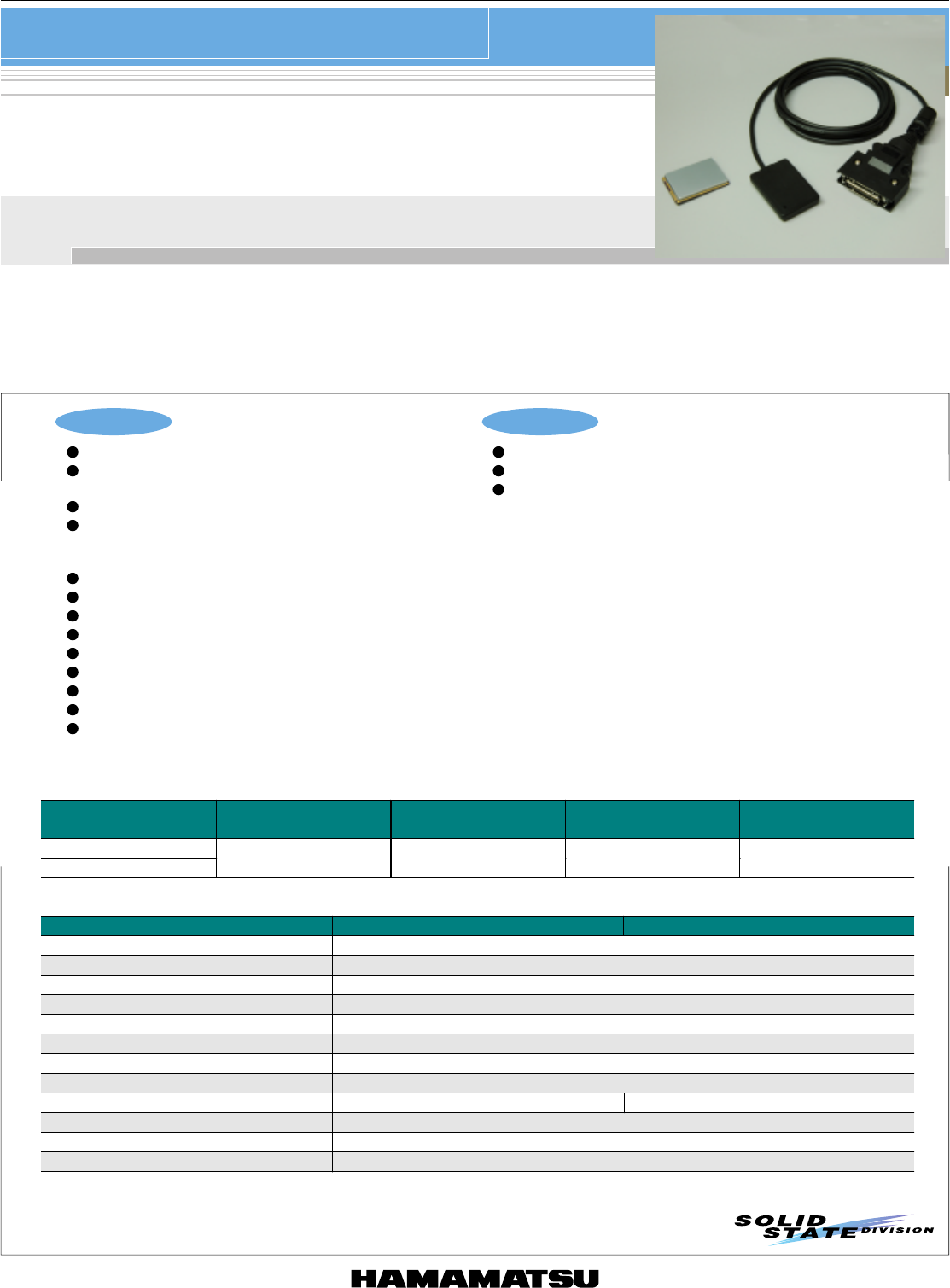
S8984 is an FFT-CCD image sensor ideal for intra-oral X-ray imaging in dental diagnosis. S8984 has about 2 mega (1700 × 1200) pixels each of
which is 20 × 20 µm. The fiber optic plate (FOP) used as an input window is as thin as 1.5 mm but highly resistant to X-ray irradiation, making
S8984 very reliable even over a long-term operation. The scintillator coated on the FOP is optimized to have high X-ray sensitivity and high
resolution (20 Lp/mm).
S8985-02 is an easy-to-use X-ray imaging module using S8984, with added functions such as a cable assembly and X-ray trigger circuit. S8985-
02 is pin compatible with S8981-02 (number of pixels is increased). S8985-02 is advanced type of S8985 and adapted both AC and DC X-ray
sources.
1
Selection guide
Type No. Cooling
Number of
total pixels
Number of
active pixels
Active area
[mm (H) × mm (V)]
S8984
S8985-02
Non-cooled 1708 × 1202 1700 × 1200 34 × 24
General ratings
Parameter S8984 S8985-02
CCD structure Full frame transfer
Fill factor 100 %
Number of active pixels 1700 (H) × 1200 (V)
Pixel size 20 (H) × 20 (V) µm
Active area 34 (H) × 24 (V) mm
Vertical clock phase 2 phase
Horizontal clock phase 2 phase
Output circuit Emitter follower without load resistance
Dimensional outline 39.5 (H) × 27.5 (V) mm 42.6 (H) × 30.6 (V) mm
Reliability 100,000 shots at 60 kVp, 30 m Roentgen
Window Scintillator on 1.5 mm FOP
Other MPP mode (low dark current operation), module (S8985-02)
CCD area image sensor
S8984, S8985-02
2
Absolute maximum ratings (Ta=25 °C)
Parameter Symbol Min. Typ. Max. Unit
Storage temperature Tstg -20 - +70 °C
Operating temperature Topr 0 - +40 °C
OD voltage V
OD
-0.5 - +20 V
RD voltage V
RD
-0.5 - +18 V
SG voltage V
SG
-15 - +15 V
OG voltage V
OG
-15 - +15 V
RG voltage V
RG
-15 - +15 V
TG voltage V
TG
-15 - +15 V
Vertical clock voltage V
P1V
, V
P2V
-15 - +15 V
Horizontal clock voltage V
P1H
, V
P2H
-15 - +15 V
Vcc voltage Vcc 0 - +7 V
Operating conditions (MPP mode, Ta=25 °C)
Parameter Symbol Min. Typ. Max. Unit
Output transistor drain voltage V
OD
12 15 - V
Reset drain voltage V
RD
12 13 14 V
Output gate voltage V
OG
-0.5 2 5 V
Substrate voltage Vss - 0 - V
High V
P1VH
, V
P2VH
0 3 6 V
Vertical shift register
clock voltage
Low V
P1VL
, V
P2VL
-9 -8 -7 V
High V
P1HH
, V
P2HH
036V
Horizontal shift register
clock voltage
Low V
P1HL
, V
P2HL
-9 -8 -7 V
High Vs
GH
0 3 6 V
Summing gate voltage
Low Vs
GL
-9 -8 -7 V
High V
RGH
036V
Reset gate voltage
Low V
RGL
-9 -8 -7 V
High V
TGH
0 3 6 V
Transfer gate voltage
Low V
TGL
-9 -8 -7 V
+5 V power supply voltage Vcc 4.75 5 5.25 V
Electrical characteristics (Ta=25 °C)
Parameter Symbol Remark Min. Typ. Max. Unit
Signal output frequency fc *
1
-15MHz
Vertical shift register capacitance C
P1
v, C
P2
v - 70,000 - pF
S8984 - 400 -
Horizontal shift
register capacitance
S8985-02
C
P1H
, C
P2H
- 600 -
pF
S8984 - 20 -
Summing gate capacitance
S8985-02
Cs
G
- 220 -
pF
S8984 - 20 -
Reset gate capacitance
S8985-02
C
RG
- 220 -
pF
S8984 - 250 -
Transfer gate capacitance
S8985-02
C
TG
- 450 -
pF
Charge transfer efficiency CTE *
2
0.99995 0.99998 - -
DC output level V
O
ut *
3
5 8 11 V
Output impedance Zo *
3
- 500 -
Power dissipation P *
3
*
4
- 75 - mW
S8984 - 1 -
+5 V power supply current
S8985-02
Icc
-2-
mA
*1: S8984 only. In case of S8985-02, maximum frequency is strongly depend on peripheral circuit and cable length.
*2: Measured at half of the full well capacity. CTE is defined per pixel.
*3: V
OD
=15 V
*4: Power dissipation of the on-chip amplifier.
CCD area image sensor
S8984, S8985-02
......
......
1
VS1 VS2 VS3 VS4
VS1199
VS1200
VS1201
VS1202
2
3
1696
1697
1698
1699
1700
23
11991198 1200
D1
D2
S1
S2
S3
S4
S5
S6
S1699
S1700
S1701
S1702
S1703
S1704
D3
D4
......
X-RAY IRRADIATION
MONITORING PHOTODIODE
PD
P1V
P2V
TG
SS
RG
OG
SG
P1H
P2H
OS
OD
RD
3
Electrical and optical characteristics (Ta=25 °C, unless otherwise noted, V
OD
=15 V)
Parameter Symbol Remark Min. Typ. Max. Unit
Vertical 100 200 -
Horizontal - 300 -Full well capacity
Summing
Fw
- 600 -
ke
-
CCD node sensitivity Sv *
5
1.0 1.4 - µV/e
-
Dark current (MPP mode) DS *
6
- 250 2,500 e
-
/pixel/s
Readout noise Nr *
7
- 60 - e
-
rms
Dynamic range DR *
8
- 3,333 - -
X-ray response non-uniformity XRNU *
9,
*
10
- ±10 ±30 %
White spots - - 20
Point
defects *
12
Black spots - - 20
Cluster defects *
13
--3
Blemish *
11
Column defects
-
*
14
--1
-
X-ray resolution
R
*
9
15 20 - Lp/mm
*5: V
OD
=15 V, R
L
(load resistance of emitter follower)=1 k
.
*6: Dark signal doubles for every 5 to 7 °C.
*7: -40 °C, operating frequency is 1 MHz.
*8: Dynamic range = Full well capacity / Readout noise
*9: X-ray irradiation of 60 kVp, measured at half of the full well capacity.
*10: XRNU (%) = Noise / Signal × 100
Noise: Fixed pattern noise (peak to peak)
In the range that excludes 5 pixels from edges to the center at every position.
*11: Refer to “Characteristics and use of FFT-CCD area image sensor” of technical information.
*12: White spots > 10 times of Max. Dark signal (2500 e
-
/pixel/s).
Black spots > 50 % reduction in response relative to adjacent pixels, measured at half of the full well capacity.
*13: continuous 2 to 9 point defects.
*14: continuous > 10 point defects.
Device structure
KMPDC0220EA
Pixel format
Left Horizontal Direction
Right
Blank
Optical
black
Isolation Effective Isolation
Optical
black
Blank
2 2 1 1700 1 0 2
Top
Vertical direction
Bottom
Isolation Effective Isolation
1 1200 1
123NEXT