Freelance Electronics Components Distributor
Closed Dec 25th-26th
800-300-1968
We Stock Hard to Find Parts

TLC555MJGB

Part # TLC555MJGB
Description IC, LOW POWER TIMER - Rail/Tube
Category Microcircuit
Availability Out of Stock
Qty 0
Qty Price
1 + $4.78750


Technical Document


DISCLAIMER: The information provided herein is solely for informational purposes. Customers must be aware of the suitability of this product for their application, and consider that variable factors such as Manufacturer, Product Category, Date Codes, Pictures and Descriptions may differ from available inventory.


 
SLFS043F − SEPTEMBER 1983 − REVISED FEBRUARY 2005
7
POST OFFICE BOX 655303 DALLAS, TEXAS 75265
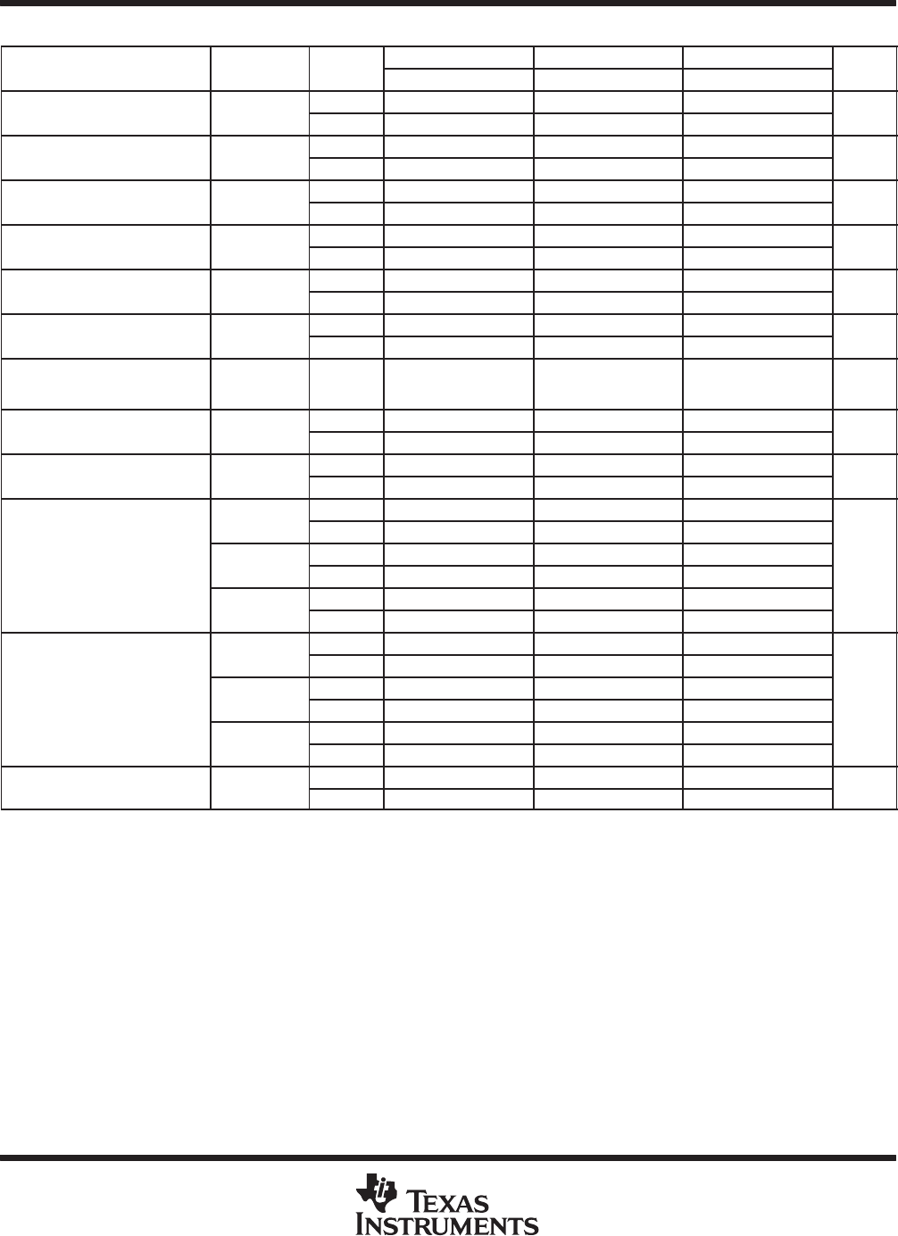
electrical characteristics at specified free-air temperature, V
DD
= 15 V
PARAMETER
TEST
CONDITIONS
T
A
TLC555C TLC555I TLC555Q, TLC555M
PARAMETER
TEST
CONDITIONS
T
A
MIN TYP MAX MIN TYP MAX MIN TYP MAX
UNIT
V
IT
Threshold voltage
25°C 9.45 10 10.55 9.45 10 10.55 9.45 10 10.55
V
IT
Threshold voltage
Full range 9.35 10.65 9.35 10.65 9.35 10.65
V
I
IT
Threshold current
25°C 10 10 10
I
IT
Threshold current
MAX 75 150 5000
pA
V
I(TRIG)
Trigger voltage
25°C 4.65 5 5.35 4.65 5 5.35 4.65 5 5.35
V
I(TRIG)
Trigger voltage
Full range 4.55 5.45 4.55 5.45 4.55 5.45
V
I
I(TRIG)
Trigger current
25°C 10 10 10
I
I(TRIG)
Trigger current
MAX 75 150 5000
pA
V
I(RESET)
Reset voltage
25°C 0.4 1.1 1.5 0.4 1.1 1.5 0.4 1.1 1.5
V
I(RESET
)
Reset voltage
Full range 0.3 1.8 0.3 1.8 0.3 1.8
V
I
I(RESET)
Reset current
25°C 10 10 10
I
I(RESET)
Reset current
MAX 75 150 5000
pA
Control voltage (open
circuit) as a percent-
age of supply voltage
MAX 66.7% 66.7% 66.7%
Discharge switch
I
OL
= 100 mA
25°C 0.77 1.7 0.77 1.7 0.77 1.7
Discharge switch
on-state voltage
I
OL
= 100 mA
Full range 1.8 1.8 1.8
V
Discharge switch
25°C 0.1 0.1 0.1
Discharge switch
off-state current
MAX 0.5 120 120
nA
I
OH
= − 10 mA
25°C 12.5 14.2 12.5 14.2 12.5 14.2
I
OH
= − 10 mA
Full range 12.5 12.5 12.5
V
OH
High-level output
I
OH
= − 5 mA
25°C 13.5 14.6 13.5 14.6 13.5 14.6
V
OH
High-level output
voltage
I
OH
= − 5 mA
Full range 13.5 13.5 13.5
V
I
OH
= − 1 mA
25°C 14.2 14.9 14.2 14.9 14.2 14.9
I
OH
= − 1 mA
Full range 14.2 14.2 14.2
I
OL
= 100 mA
25°C 1.28 3.2 1.28 3.2 1.28 3.2
I
OL
= 100 mA
Full range 3.6 3.7 3.8
V
OL
Low-level output
I
OL
= 50 mA
25°C 0.63 1 0.63 1 0.63 1
V
OL
Low-level output
voltage
I
OL
= 50 mA
Full range 1.3 1.4 1.5
V
I
OL
= 10 mA
25°C 0.12 0.3 0.12 0.3 0.12 0.3
I
OL
= 10 mA
Full range 0.4 0.4 0.45
I
DD
Supply current
See Note 2
25°C 360 600 360 600 360 600
I
DD
Supply current See Note 2
Full range 800 900 1000
µA
Full range is 0°C to 70°C for TLC555C, −40°C to 85°C for TLC555I, −40°C to 125°C for the TLC555Q, and −55°C to 125°C for TLC555M. For
conditions shown as MAX, use the appropriate value specified in the recommended operating conditions table.
NOTE 2: These values apply for the expected operating configurations in which THRES is connected directly to DISCH or TRIG.

 
SLFS043F − SEPTEMBER 1983 − REVISED FEBRUARY 2005
8
POST OFFICE BOX 655303 DALLAS, TEXAS 75265
operating characteristics, V
DD
= 5 V, T
A
= 25°C (unless otherwise noted)
PARAMETER
TEST CONDITIONS MIN TYP MAX UNIT
Initial error of timing interval
V
DD
= 5 V to 15 V,
R
A
= R
B
= 1 k
to 100 k
,
1% 3%
Supply voltage sensitivity of timing interval
V
DD
= 5 V to 15 V,
C
T
= 0.1 µF,
R
A
= R
B
= 1 k to 100 k,
See Note 3
0.1 0.5 %/V
t
r
Output pulse rise time
R
L
= 10 M
C
L
= 10 pF
20 75
ns
t
f
Output pulse fall time
R
L
= 10 MΩ, C
L
= 10 pF
15 60
ns
f
max
Maximum frequency in astable mode
R
A
= 470 Ω,
C
T
= 200 pF,
R
B
= 200 Ω,
See Note 3
1.2 2.1 MHz
Timing interval error is defined as the difference between the measured value and the average value of a random sample from each process
run.
NOTE 3: R
A
, R
B
, and C
T
are as defined in Figure 1.
electrical characteristics at V
DD
= 5 V, T
A
= 25°C
PARAMETER
TEST CONDITIONS MIN TYP MAX UNIT
V
IT
Threshold voltage 2.8 3.3 3.8 V
I
IT
Threshold current 10 pA
V
I(TRIG)
Trigger voltage 1.36 1.66 1.96 V
I
I(TRIG)
Trigger current 10 pA
V
I(RESET)
Reset voltage 0.4 1.1 1.5 V
I
I(RESET)
Reset current 10 pA
Control voltage (open circuit) as a percentage of supply voltage 66.7%
Discharge switch on-state voltage I
OL
= 10 mA 0.14 0.5 V
Discharge switch off-state current 0.1 nA
V
OH
High-level output voltage I
OH
= − 1 mA 4.1 4.8 V
I
OL
= 8 mA 0.21 0.4
V
OL
Low-level output voltage
I
OL
= 5 mA 0.13 0.3
V
V
OL
Low-level output voltage
I
OL
= 3.2 mA 0.08 0.3
V
I
DD
Supply current See Note 2 170 350 µA
NOTE 2: These values apply for the expected operating configurations in which THRES is connected directly to DISCH or TRIG.

 
SLFS043F − SEPTEMBER 1983 − REVISED FEBRUARY 2005
9
POST OFFICE BOX 655303 DALLAS, TEXAS 75265
TYPICAL CHARACTERISTICS
Figure 1
2
1
−75 − 50 − 25 0 25 75 125
Discharge Switch On-State Resistance −
DISCHARGE SWITCH ON-STATE RESISTANCE
vs
FREE-AIR TEMPERATURE
50 100
10
4
20
100
40
7
70
T
A
− Free-Air Temperature − °C
V
DD
= 2 V, I
O
= 1 mA
V
DD
= 5 V, I
O
= 10 mA
V
DD
= 15 V, I
O
= 100 mA
Figure 2
100
0
0 2 4 6 8 12 16
PROPAGATION DELAY TIMES TO DISCHARGE
OUTPUT FROM TRIGGER AND THRESHOLD
SHORTED TOGETHER
vs
SUPPLY VOLTAGE
10 14
400
200
500
600
300
V
DD
− Supply Voltage − V
2018
PHL
t,
PLH
t − Propagation Delay Times − ns
t
PLH
I
O(on)
1 mA
C
L
0
T
A
= 25°C
The effects of the load resistance on these values must be
taken into account separately.
t
PHL
APPLICATION INFORMATION
0.1 µF
0.1 µF
C
T
C
L
R
L
Output
R
B
R
A
GND
TRIG
THRES
RESET
DISCH
CONT V
DD
OUT
V
DD
2/3 V
DD
1/3 V
DD
GND
t
PHL
t
PLH
t
c(H)
t
c(L)
CIRCUIT
TRIGGER
AND
THRESHOLD
VOLTAGE
WAVEFORM
TLC555
6
1
3
85
4
7
2
Pin
numbers
shown
are
for
all
packages
except
the
FK
package.
Figure 3. Astable Operation
PREVIOUS1234567NEXT