Closed Dec 25th-26th
800-300-1968
We Stock Hard to Find Parts
My Account
|
My Orders
|
My Cart
Questions?
(800) 300-1968
Register
(current)
My Account
(current)
My Orders
(current)
My Cart
(current)
Categories
(current)
Manufacturers
Request a Quote
Sell Your Excess
Consignment
Quality Assurance
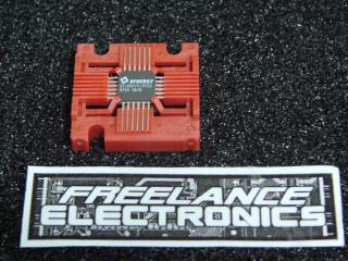
SY100EL92ZC
Part #
SY100EL92ZC
Description
IC XLATOR LV/PECL TRPL 20SOIC
Category
Microcircuit
Availability
Out of Stock
Qty
0
Qty
Price
1 +
$3.03360
Related Items
Generic
IC
SY1001E131JC
Generic
IC
SY100474-5FCS
Generic
IC
SY100E016JC
$7.55392
Generic
IC
SY100E111JC
$6.85697
Generic
IC
SY100E137JC
$11.53982
Generic
IC
SY100E150JC
$6.35215