Freelance Electronics Components Distributor
Closed Dec 25th-26th
800-300-1968
We Stock Hard to Find Parts

OP27AJ

Part # OP27AJ
Description Operational Amplifiers - Op Amps
Category Microcircuit
Availability In Stock
Qty 1
Qty Price
1 + $31.30939
Manufacturer Available Qty
PMI
Date Code: 8944
  • Shipping Freelance Stock: 1
    Ships Immediately


Technical Document


DISCLAIMER: The information provided herein is solely for informational purposes. Customers must be aware of the suitability of this product for their application, and consider that variable factors such as Manufacturer, Product Category, Date Codes, Pictures and Descriptions may differ from available inventory.

REV. A
OP27
–10–
TOTAL SUPPLY VOLTAGE V
OPEN-LOOP GAIN V/V
2.5
010 40
20 30
T
A
= 25C
50
2.0
1.5
1.0
0.5
0
R
L
= 2k
R
L
= 1k
TPC 19. Open-Loop Voltage Gain vs.
Supply Voltage
CAPACITIVE LOAD pF
% OVERSHOOT
80
60
0
0 500 2000
1000 1500
40
20
V
S
= 15V
V
IN
= 100mV
A
V
= +1
100
2500
TPC 22. Small-Signal Overshoot vs.
Capacitive Load
TIME FROM OUTPUT SHORTED TO
GROUND Min
SHORT-CIRCUIT CURRENT mA
60
01 4
23 5
50
40
30
20
10
T
A
= 25C
V
S
= 15V
I
SC
(+)
I
SC
()
TPC 25. Short-Circuit Current vs.
Time
FREQUENCY Hz
28
1k 10k 100k 1M
PEAK-TO-PEAK AMPLITUDE V
24
20
16
12
8
4
0
T
A
= 25C
V
S
= 15V
10M
TPC 20. Maximum Output Swing vs.
Frequency
20mV
500ns
50mV
0V
50mV
A
VCL
= +1
C
L
= 15pF
V
S
= 15V
T
A
= 25C
TPC 23. Small-Signal Transient
Response
FREQUENCY Hz
CMRR dB
140
1k
120
100
80
60
10k 100k 1M100
V
S
= 15V
T
A
= 25C
V
CM
= 10V
TPC 26. CMRR vs. Frequency
LOAD RESISTANCE
MAXIMUM OUTPUT V
18
100
1k 10k
16
14
12
10
8
6
4
2
0
2
T
A
= 25
C
V
S
=
15V
POSITIVE
SWING
NEGATIVE
SWING
TPC 21. Maximum Output Voltage
vs. Load Resistance
2V
2
s
+5V
0V
5V
A
VCL
= +1
V
S
= 15V
T
A
= 25C
TPC 24. Large-Signal Transient
Response
SUPPLY VOLTAGE V
COMMON-MODE RANGE V
16
0 5
12
8
4
0
4
10 15 20
8
12
16
T
A
= 55C
T
A
= +125C
T
A
= +25C
T
A
= +25C
T
A
= 55C
T
A
= +125C
TPC 27. Common-Mode Input Range
vs. Supply Voltage
REV. A
–11–
OP27
OP12
OP27
D.U.T.
100k
4.3k
4.7F
2k
24.3k
VO LTAG E
GAIN
= 50,000
2.2F
22F
110k
SCOPE 1
R
IN
= 1M
0.1F
10
100k
0.1F
TPC 28. Voltage Noise Test Circuit
(0.1 Hz to 10 Hz)
LOAD RESISTANCE
2.4
100 1k 10k 100k
OPEN-LOOP VOLTAGE GAIN V/V
T
A
= 25C
V
S
= 15V
2.2
2.0
1.8
1.6
1.4
1.2
1.0
0.8
0.6
0.4
TPC 29. Open-Loop Voltage Gain vs.
Load Resistance
1 SEC/DIV
120
80
40
0
40
90
120
VOLTAGE NOISE nV
0.1Hz to 10Hz p-p NOISE
TPC 30. Low-Frequency Noise
APPLICATION INFORMATION
OP27 series units may be inserted directly into 725 and OP07
sockets with or without removal of external compensation or
nulling components. Additionally, the OP27 may be fitted to
unnulled 741-type sockets; however, if conventional 741 nulling
circuitry is in use, it should be modified or removed to ensure
correct OP27 operation. OP27 offset voltage may be nulled to
zero (or another desired setting) using a potentiometer (see
Offset Nulling Circuit).
The OP27 provides stable operation with load capacitances of
up to 2000 pF and ±10 V swings; larger capacitances should be
decoupled with a 50 resistor inside the feedback loop. The
OP27 is unity-gain stable.
Thermoelectric voltages generated by dissimilar metals at the
input terminal contacts can degrade the drift performance. Best
operation will be obtained when both input contacts are main-
tained at the same temperature.
OFFSET VOLTAGE ADJUSTMENT
The input offset voltage of the OP27 is trimmed at wafer level.
However, if further adjustment of V
OS
is necessary, a 10 k trim
potentiometer can be used. TCV
OS
is not degraded (see Offset
Nulling Circuit). Other potentiometer values from 1 k to 1 M
can be used with a slight degradation (0.1 µV/°C to 0.2 µV/°C)
of TCV
OS
. Trimming to a value other than zero creates a drift of
approximately (V
OS
/300) µV/°C. For example, the change in
TCV
OS
will be 0.33 µV/°C if V
OS
is adjusted to 100 µV. The
offset voltage adjustment range with a 10 k potentiometer is
±4 mV. If smaller adjustment range is required, the nulling
sensitivity can be reduced by using a smaller pot in conjuction
with fixed resistors. For example, the network below will have a
±280 µV adjustment range.
1
84.7k4.7k 1kPOT
V+
Figure 2.
NOISE MEASUREMENTS
To measure the 80 nV peak-to-peak noise specification of the
OP27 in the 0.1 Hz to 10 Hz range, the following precautions
must be observed:
1. The device must be warmed up for at least five minutes.
As shown in the warm-up drift curve, the offset voltage
typically changes 4 µV due to increasing chip temperature
after power-up. In the 10-second measurement interval,
these temperature-induced effects can exceed tens-of-
nanovolts.
2. For similar reasons, the device has to be well-shielded from
air currents. Shielding minimizes thermocouple effects.
FREQUENCY Hz
POWER SUPPLY REJECTION RATIO dB
140
1
T
A
= 25C
120
100
80
60
40
20
0
10 100 1k 10k 100k 1M 10M 100M
160
POSITIVE
SWING
NEGATIVE
SWING
TPC 31. PSRR vs. Frequency
REV. A
OP27
–12–
3. Sudden motion in the vicinity of the device can also
“feedthrough” to increase the observed noise.
4. The test time to measure 0.1 Hz to 10 Hz noise should not
exceed 10 seconds. As shown in the noise-tester frequency
response curve, the 0.1 Hz corner is defined by only one
zero. The test time of 10 seconds acts as an additional zero
to eliminate noise contributions from the frequency band
below 0.1 Hz.
5. A noise-voltage-density test is recommended when measuring
noise on a large number of units. A 10 Hz noise-voltage-
density measurement will correlate well with a 0.1 Hz to 10 Hz
peak-to-peak noise reading, since both results are determined
by the white noise and the location of the 1/f corner frequency.
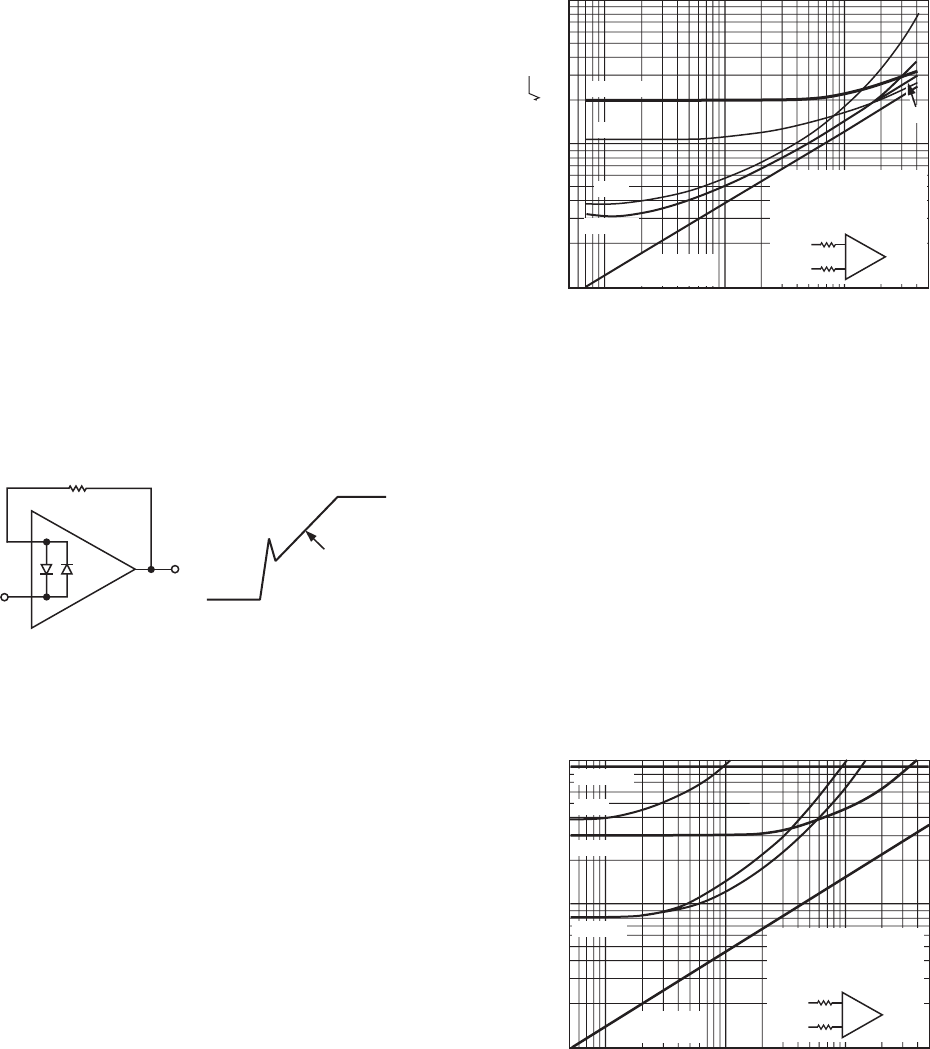
UNITY-GAIN BUFFER APPLICATIONS
When R
f
100 and the input is driven with a fast, large signal
pulse (>1 V), the output waveform will look as shown in the
pulsed operation diagram (Figure 3).
During the fast feedthrough-like portion of the output, the input
protection diodes effectively short the output to the input and a
current, limited only by the output short-circuit protection, will
be drawn by the signal generator. With R
f
500 , the output is
capable of handling the current requirements (I
L
20 mA at 10 V);
the amplifier will stay in its active mode and a smooth transition
will occur.
When R
f
> 2 k, a pole will be created with R
f
and the amplifier’s
input capacitance (8 pF) that creates additional phase shift and
reduces phase margin. A small capacitor (20 pF to 50 pF) in
parallel with R
f
will eliminate this problem.
+
OP27
R
f
2.8V/s
Figure 3. Pulsed Operation
COMMENTS ON NOISE
The OP27 is a very low-noise monolithic op amp. The outstanding
input voltage noise characteristics of the OP27 are achieved mainly
by operating the input stage at a high quiescent current. The input
bias and offset currents, which would normally increase, are held
to reasonable values by the input bias-current cancellation circuit.
The OP27A/E has I
B
and I
OS
of only ±40 nA and 35 nA at 25°C
respectively. This is particularly important when the input has a
high source resistance. In addition, many audio amplifier design-
ers prefer to use direct coupling. The high I
B
, V
OS
, and TCV
OS
of previous designs have made direct coupling difficult, if not
impossible, to use.
Voltage noise is inversely proportional to the square root of bias
current, but current noise is proportional to the square root of
bias current. The OP27’s noise advantage disappears when high
source-resistors are used. Figures 4, 5, and 6 compare OP27’s
observed total noise with the noise performance of other devices
in different circuit applications.
Total Noise
Voltage Noise
Current Noise R
sistor Noise
S
=
()
+
×
()
+
()
2
2
2
12
Re
/
Figure 4 shows noise versus source-resistance at 1000 Hz. The
same plot applies to wideband noise. To use this plot, multiply
the vertical scale by the square root of the bandwidth.
R
S
SOURCE RESISTANCE
10
50 10k
TOTAL NOISE nV/ Hz
5
500 1k 5k
1
100
50
100 50k
R
S1
R
S2
1 R
S
UNMATCHED
e.g. R
S
= R
S1
= 10k, R
S2
= 0
2 R
S
MATCHED
e.g. R
S
= 10k, R
S1
= R
S2
= 5k
OP07
5534
OP27/37
REGISTER
NOISE ONLY
OP08/108
1
2
Figure 4. Noise vs. Source Resistance (Including Resistor
Noise) at 1000 Hz
At R
S
<1 k, the OP27s low voltage noise is maintained. With
R
S
<1 k, total noise increases, but is dominated by the resis-
tor noise rather than current or voltage noise. lt is only beyond
R
S
of 20 k that current noise starts to dominate. The argument
can be made that current noise is not important for applica-
tions with low to moderate source resistances. The crossover
between the OP27, OP07, and OP08 noise occurs in the 15 k to
40 k region.
Figure 5 shows the 0.1 Hz to 10 Hz peak-to-peak noise. Here
the picture is less favorable; resistor noise is negligible and current
noise becomes important because it is inversely proportional to
the square root of frequency. The crossover with the OP07
occurs in the 3 k to 5 k range depending on whether bal-
anced or unbalanced source resistors are used (at 3 k the I
B
and I
OS
error also can be three times the V
OS
spec.).
R
S
SOURCE RESISTANCE
100
50 10k
p-p NOISE nV
50
500 1k 5k
10
1k
500
100 50k
R
S1
R
S2
1 R
S
UNMATCHED
e.g. R
S
= R
S1
= 10k, R
S2
= 0
2 R
S
MATCHED
e.g. R
S
= 10k, R
S1
= R
S2
= 5k
OP07
5534
OP27/37
REGISTER
NOISE ONLY
OP08/108
1
2
Figure 5. Peak-to-Peak Noise (0.1 Hz to 10 Hz) as Source
Resistance (Includes Resistor Noise)
PREVIOUS123456NEXT